Page 20 of 35
Design Guideline for making VR circuitry :
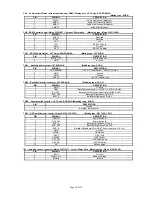
CNB1 – Backlight inverter connector: JST S5B-XH-A (Matching type : XHP-5)
PIN SYMBOL
DESCRIPTION
1 GND
Ground
2
VBKL
Backlight power supply, +12VDC / +24V DC, 3A max
3
BLCTRL
Backlight On/Off control signal (refer to JB2 & JB3)
4
BVR_WIP
Backlight brightness VR pin WIP
5
BVR_A
Backlight brightness VR pin A
CNC1 – OSD switch mount control, Hirose DF13A-12P-1.25H (Mating type : DF13-12S-1.25C)
PIN SYMBOL
DESCRIPTION
1
PSWIN
Power button A
2
SW_ON
Power button B
3
BVR_A
Backlight Brightness VR pin A
4
BVR_WIP
Backlight Brightness R pin WIP
5
BVR_B
Backlight Brightness VR pin B (470 ohm resistor to +5V Vcc)
6 GND
Ground
7
MENU
OSD menu
8 -/LEFT
OSD
-/Left
9 +/RIGHT
OSD
+/Right
10
SEL_DN
OSD Select down
11
SEL_UP
OSD Select up
12 NC
No
connection
The VR for brightness depends on the inverter. The main power load for On/Off is handled by a relay on the controller.
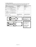
Example for circuit design :
Signal description / Notes :
1) R1 : 470ohm on board
2) RPOT is an external potentiometer (in-line dip
style) that can be plugged directly into CNC1 pins
3,4,5. RPOT must be supplied / installed by user.
3) BVR_B : Voltage tapped from “top” of
potentiometer, the node of R1 and RPOT.
4) BVR_WIP : Voltage tapped from wiper arm of
RPOT.
5) BVR_A : Voltage tapped from “bottom” of
RPOT.
Note : BVR_A voltage is left floating on the
controller board. To use this circuit, you need
to tie this point to a potential (usually GND,
available at CNC1 pin 6).
1.)Choose RPOT = 10K
2.) Tie BVR_A to GND
3.) Circuit analysis gives BVR_WIP as the
following (see Figure 1)
BVR_WIP = 5 x (Rbc/10.47)
where BVR_WIP is in Volts.
And Rbc is the resistance from the wiper arm
to bottom of pot in Kohms.
To evaluate, plug in different values of Rbc :
Rbc BVR_WIP
0
0 V
2.5 K
1.2 V
5 K
2.4 V
7.5 K
3.6 V
10 K
4.8 V
So this circuit could provide Brightness
adjust voltage ranging from 0V to 5V.

