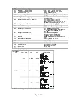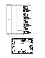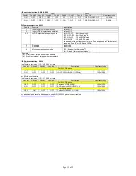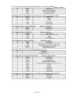
Page 16 of 35
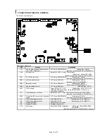
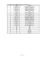
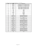
J3 – LVDS output connector: JAE FI-RE51S-HF (Matching type : JAE FI-RE51HL)
PIN SYMBOL
DESCRIPTION
1
VLCD_HV
Panel power supply (+12V / 18V) (selected by JA3 & JA6)
2
VLCD_HV
Panel power supply (+12V / 18V) (selected by JA3 & JA6)
3
VLCD_HV
Panel power supply (+12V / 18V) (selected by JA3 & JA6)
4
VLCD_HV
Panel power supply (+12V / 18V) (selected by JA3 & JA6)
5
VLCD_HV
Panel power supply (+12V / 18V) (selected by JA3 & JA6)
6
VLCD_LV
Panel power supply (3,3V/5V) (selected by JA3 & JA6)
7 VLCD_LV
Panel power supply (3,3V/5V) (selected by JA3 & JA6)
8 VLCD_LV
Panel power supply (3,3V/5V) (selected by JA3 & JA6)
9 VLCD_LV
Panel power supply (3,3V/5V) (selected by JA3 & JA6)
10 VLCD_LV
Panel power supply (3,3V/5V) (selected by JA3 & JA6)
11 GND
Ground
12 GND
Ground
13 GND
Ground
14 GND
Ground
15 GND
Ground
16 LVDS_SEL
Reserved
17 BIT_SEL
Reserved
18 TP6
Reserved
19 TP7
Reserved
20 GND
Ground
21 GND
Ground
22
LVDS_
Positive differential LVDS data bit A4
23
LVDS_OUT1_A4-
Negative differential LVDS data bit A4
24
LVDS_
Positive differential LVDS data bit A3
25
LVDS_OUT1_A3-
Negative differential LVDS data bit A3
26 GND
Ground
27
LVDS_
Positive LVDS clock for A channel
28
LVDS_OUT1_AC-
Negative LVDS clock for A channel
29 GND
Ground
30
LVDS_
Positive differential LVDS data bit A2
31
LVDS_OUT1_A2-
Negative differential LVDS data bit A2
32
LVDS_
Positive differential LVDS data bit A1
33
LVDS_OUT1_A1-
Negative differential LVDS data bit A1
34
LVDS_
Positive differential LVDS data bit A0
35
LVDS_OUT1_A0-
Negative differential LVDS data bit A0
36 GND
Ground
37
LVDS_
Positive differential LVDS data bit B4
38
LVDS_OUT1_B4-
Negative differential LVDS data bit B4
39
LVDS_
Positive differential LVDS data bit B3
40
LVDS_OUT1_B3-
Negative differential LVDS data bit B3
41 GND
Ground
42
LVDS_
Positive LVDS clock for B channel
43
LVDS_OUT1_BC-
Negative LVDS clock for B channel
44 GND
Ground
45
LVDS_
Positive differential LVDS data bit B2
46
LVDS_OUT1_B2-
Negative differential LVDS data bit B2
47
LVDS_
Positive differential LVDS data bit B1
48
LVDS_OUT1_B1-
Negative differential LVDS data bit B1
49
LVDS_
Positive differential LVDS data bit B0
50
LVDS_OUT1_B0-
Negative differential LVDS data bit B0
51 GND
Ground

