61
DVD-2910/955
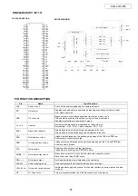
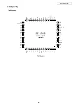
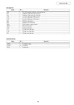
Differential Signal Data Pins
Pin Name
Pin #
Type
Description
TX0+
TX0-
TX1+
TX1-
TX2+
TX2-
25
24
28
27
31
30
Analog
Analog
Analog
Analog
Analog
Analog
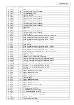
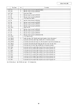
TMDS Low Voltage Differential Signal output data pairs.
These pins are tri-stated when PD# is asserted.
TXC+
TXC-
22
21
Analog
Analog
TMDS Low Voltage Differential Signal output clock pairs.
These pins are tri-stated when PD# is asserted.
EXT_SWING
19
Analog Voltage Swing Adjust. A resistor should tie this pin to AVCC. This resistor
determines the amplitude of the voltage swing. A 510 ohm resistor is
recommended for remote display applications. For notebook computers, 680 ohm
is recommended.
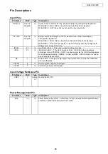
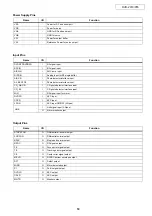
Configuration/Programming Pins
Pin Name
Pin #
Type
Description
MSEN
11
Out
Monitor Sense. This pin is an open collector output. The output is programmable
through the I
2
C interface (see I
2
C register definitions). An external 5K pull-up
resistor is required on this pin.
RESERVED
34
In
This pin is reserved.
NC
7,8
NC
These pins are not electrically connected inside the package.
Control Pins
These control pins allow configuration of the transmitter through the slave I
2
C port, which is required by HDCP.
Pin Name
Pin #
Type
Description
ISEL/RST#
13
In
I
2
C Interface Select. If HIGH, then the I
2
C interface is active.
SCLS
15
In
DDC I
2
C Clock.
SDAS
14
In/Out
DDC I
2
C Data.
CTL3
6
In
External CTL3.
HTPLG
9
In
Monitor Charge Input. This pin is used to connect to the DVI Hot Plug pin to detect
the presence of an attached monitor.
Power and Ground Pins
Pin Name
Pin #
Type Description
VCC
1,12,33
Power
Digital VCC. Connect to 3.3V supply.
GND
16,35,64
Ground
Digital GND.
AVCC
23,29
Power
Analog VCC. Connect to 3.3V supply.
AGND
20,26,32
Ground
Analog GND.
PVCC1
18
Power
Primary PLL Analog VCC. Connect to regulated 3.3V supply.
PVCC2
49
Power
Filter PLL Analog VCC. Connect to regulated 3.3V supply.
PGND1
17
Ground
PLL Analog GND.
PGND2
48
Ground
PLL Analog GND.
Summary of Contents for DVD-2910
Page 29: ...29 DVD 2910 955 BLOCK DIAGRAM ...
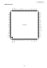
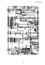
Page 48: ...48 DVD 2910 955 CXD2753R IC602 Pin Assignment Block Diagram ...
Page 79: ...79 DVD 2910 955 TA76432FC IC902 PC123 IC909 COLLECTOR EMITTER ANODE CATHODE TOP VIEW ...
Page 81: ...81 DVD 2910 955 PRINTED WIRING BORDS GU 3612 MAIN PWB P W B UNIT ASS Y COMPONENT SIDE ...
Page 82: ...82 DVD 2910 955 GU 3612 MAIN PWB P W B UNIT ASS Y FOIL SIDE ...
Page 83: ...83 DVD 2910 955 GU 3615 VODEO P W B UNIT ASS Y COMPONENT SIDE ...
Page 84: ...84 DVD 2910 955 GU 3615 VODEO P W B UNIT ASS Y FOIL SIDE ...
Page 85: ...85 DVD 2910 955 GU 3616 AUDIO POWER P W B UNIT ASS Y COMPONENT SIDE ...
Page 86: ...86 DVD 2910 955 GU 3616 AUDIO POWER P W B UNIT ASS Y FOIL SIDE ...
Page 117: ...DVD 2910 955 117 GU 3615 1 VIDEO P W B V6 V7 V8 V1 V2 V3 V4 V5 ...

