49
DVD-2910/955
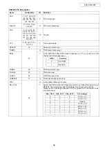
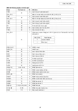
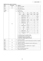
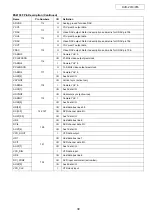
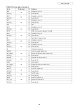
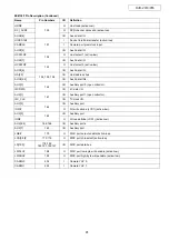
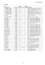
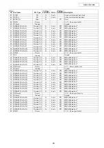
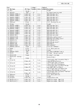
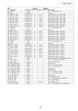
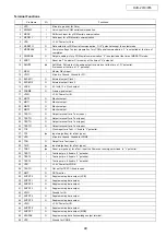
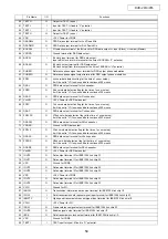
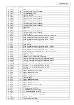
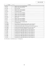
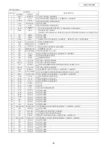
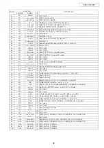
Terminal Functions
Pin Name
I/O
Functions
1
VSC
-
It fixed to ground.( for Core)
2
XMSLAT
I
Latch input for
µ
COM serial communication.
3
MSCK
I
Shift clock input for
µ
COM serial communication.
4
MSDATI
I
Data input for
µ
COM serial communication.
5
VDC
-
+2.5V Power for Core.
6
MSDATO
O
Data output for
µ
COM serial communication. “Hi-Z” potential except the output mode.
7
MSREADY
O
Completion flag of output preparation for
µ
COM serial communication. “L” is outputted at the time of
completion.
8
XMSDOE
O
Output enable pin for
µ
COM serial communication. “L” is outputted at the time of MSDATO mode.
9
XRST
I
Reset pin. The whole IC is reset by at the time of “L” potential.
10
SMUTE
Ipd
Soft Mute. Soft mute of the audio output is carried out at the time of “H” potential.
It releases at the time of “L” potential.
11
MCKI
I
Master Clock input.
12
VSIO
-
It fixed to Ground. Ground for I/O.
13
EXCKO1
O
External output Clock 1.
14
EXCKO2
O
External output Clock 2.
15
LRCK
O
44.1kHz, 1Fs Clock output.
16
FRAME
O
Frame signal output.
17
VDIO
-
+3.3V Power for I/O.
18
MNT0
O
Monitor output.
19
MNT1
O
Monitor output.
20
MNT2
O
Monitor output.
21
MNT3
O
Monitor output.
22
TESTO
O
Output terminal for a Test. (open)
23
TESTO
O
Output terminal for a Test.(open)
24
TESTO
O
Output terminal for a Test.(open)
25
TESTO
O
Output terminal for a Test.(open)
26
TCK
I
Clock input for a Test. It fixed to “L” potential.
27
TDI
Ipu
Input pin(pull-up) for a Test.(open)
28
VSC
-
It fixed to Ground. Ground for CORE.
29
TDO
O
Output for a Test.(open).
30
TMS
Ipu
Input pin(pull-up) for a Test.(open)
31
TRST
Ipu
Reset pin(pull-up) for a Test. Input the Power-on reset signal or fixed to “L” potential.
32
TEST1
I
Test input pin. It fixed to “L” potential.
33
TEST2
I
Test input pin. It fixed to “L” potential.
34
TEST3
I
Test input pin. It fixed to “L” potential.
35
VDC
-
+2.5V Power for CORE.
36
TESTO
O
Out put for TEST. It fixed to open.
37
XBIT
O
DST monitor.
38
SUPDT0
O
Supplementary data output. (LSB)
39
SUPDT1
O
Supplementary data output.
40
SUPDT2
O
Supplementary data output.
41
SUPDT3
O
Supplementary data output.
42
VSIO
-
Ground for I/O.
43
SUPDT4
O
Supplementary data output.
44
SUPDT5
O
Supplementary data output.
45
VDIO
-
+3.3V Power for I/O.
46
SUPDT6
O
Supplementary data output.
47
SUPDT7
O
Supplementary data output. (MSB)
48
XSUPAK
O
Supplementary data Acknowledge output terminal.
49
VSC
-
Ground for CORE.
Summary of Contents for DVD-2910
Page 29: ...29 DVD 2910 955 BLOCK DIAGRAM ...
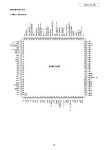
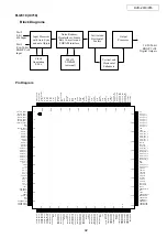
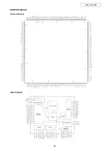
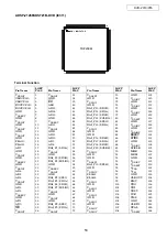
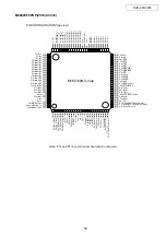
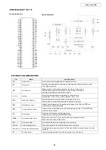
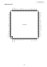
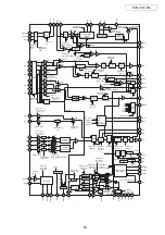
Page 48: ...48 DVD 2910 955 CXD2753R IC602 Pin Assignment Block Diagram ...
Page 79: ...79 DVD 2910 955 TA76432FC IC902 PC123 IC909 COLLECTOR EMITTER ANODE CATHODE TOP VIEW ...
Page 81: ...81 DVD 2910 955 PRINTED WIRING BORDS GU 3612 MAIN PWB P W B UNIT ASS Y COMPONENT SIDE ...
Page 82: ...82 DVD 2910 955 GU 3612 MAIN PWB P W B UNIT ASS Y FOIL SIDE ...
Page 83: ...83 DVD 2910 955 GU 3615 VODEO P W B UNIT ASS Y COMPONENT SIDE ...
Page 84: ...84 DVD 2910 955 GU 3615 VODEO P W B UNIT ASS Y FOIL SIDE ...
Page 85: ...85 DVD 2910 955 GU 3616 AUDIO POWER P W B UNIT ASS Y COMPONENT SIDE ...
Page 86: ...86 DVD 2910 955 GU 3616 AUDIO POWER P W B UNIT ASS Y FOIL SIDE ...
Page 117: ...DVD 2910 955 117 GU 3615 1 VIDEO P W B V6 V7 V8 V1 V2 V3 V4 V5 ...

