

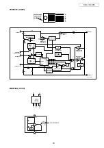

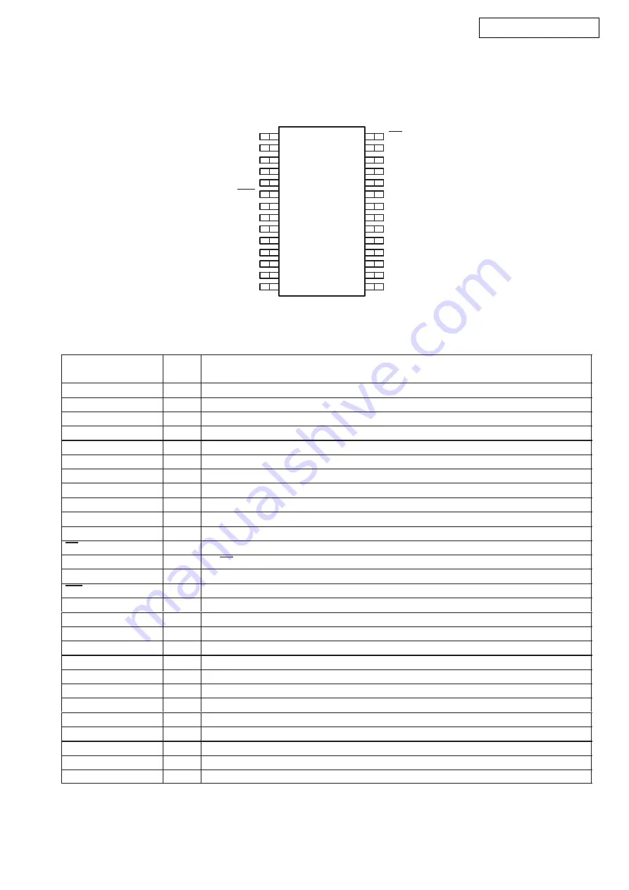
74
DVD-2910/955
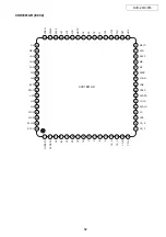
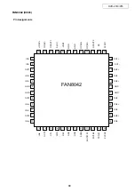
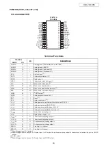
PCM1796 (IC301, 304, 307, 310)
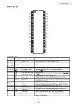
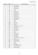
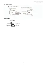
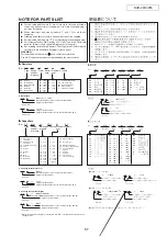
PIN ASSIGNMENTS
1
2
3
4
5
6
7
8
9
10
11
12
13
14
28
27
26
25
24
23
22
21
20
19
18
17
16
15
LRCK
BCK
DATA
MUTE
SCK
RST
V
DD
DGND
AGNDF
V
CC
R
AGNDR
V
OUT
R−
V
OUT
R+
V
COM
MS
MC
MDI
MDO
MSEL
ZEROL
ZEROR
V
CC
F
V
CC
L
AGNDL
V
OUT
L−
V
OUT
L+
AGNDC
V
CC
C
PCM1791A
(TOP VIEW)
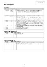
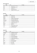
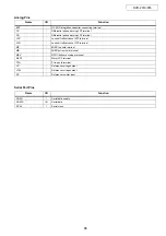
Terminal Functions
TERMINAL
I/O
DESCRIPTIONS
NAME
PIN
I/O
DESCRIPTIONS
AGNDC
16
−
Analog ground (internal bias and current DAC)
AGNDF
9
−
Analog ground (DACFF)
AGNDL
19
−
Analog ground (L-channel I/V)
AGNDR
11
−
Analog ground (R-channel I/V)
BCK
2
I
Bit clock input (1)
DATA
3
I
Serial audio data input (1)
DGND
8
−
Digital ground
LRCK
1
I
Left and right clock (fS) input (1)
MC
27
I
Mode control clock input (1)
MDI
26
I/O
Mode control data input (2)
MDO
25
O
Mode control readback data output (3)
MS
28
I/O
Mode control chip select input (4)
MSEL
24
I
I2C/SPI select (1)
MUTE
4
I
Analog output mute control (1)
RST
6
I
Reset (1)
SCK
5
I
System clock input (1)
VCCC
15
−
Analog power supply (internal bias and current DAC), 5 V
VCCF
21
−
Analog power supply (DACFF), 5 V
VCCL
20
−
Analog power supply (L-channel I/V), 5 V
VCCR
10
−
Analog power supply (R-channel I/V), 5 V
VCOM
14
−
Internal bias decoupling pin
VDD
7
−
Digital power supply, 3.3 V
VOUTL+
17
O
L-channel analog voltage
VOUTL–
18
O
L-channel analog voltage output –
VOUTR+
13
O
R-channel analog voltage
VOUTR–
12
O
R-channel analog voltage output –
ZEROL
23
O
Zero flag for L-channel
ZEROR
22
O
Zero flag for R-channel
(1) Schmitt-trigger input, 5-V tolerant
(2) Schmitt-trigger input and output. 5-V tolerant input. In I2C mode, this pin becomes an open-drain 3-state output; otherwise, this pin is a CMOS
output.
(3) 3-state output
(4) Schmitt-trigger input and output. 5-V tolerant input and CMOS output
Summary of Contents for DVD-2910
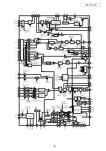
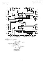
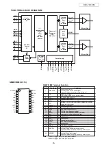
Page 29: ...29 DVD 2910 955 BLOCK DIAGRAM ...
Page 48: ...48 DVD 2910 955 CXD2753R IC602 Pin Assignment Block Diagram ...
Page 79: ...79 DVD 2910 955 TA76432FC IC902 PC123 IC909 COLLECTOR EMITTER ANODE CATHODE TOP VIEW ...
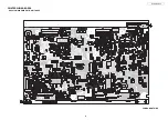
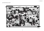
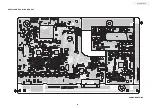
Page 81: ...81 DVD 2910 955 PRINTED WIRING BORDS GU 3612 MAIN PWB P W B UNIT ASS Y COMPONENT SIDE ...
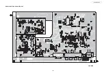
Page 82: ...82 DVD 2910 955 GU 3612 MAIN PWB P W B UNIT ASS Y FOIL SIDE ...
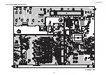
Page 83: ...83 DVD 2910 955 GU 3615 VODEO P W B UNIT ASS Y COMPONENT SIDE ...
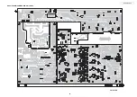
Page 84: ...84 DVD 2910 955 GU 3615 VODEO P W B UNIT ASS Y FOIL SIDE ...
Page 85: ...85 DVD 2910 955 GU 3616 AUDIO POWER P W B UNIT ASS Y COMPONENT SIDE ...
Page 86: ...86 DVD 2910 955 GU 3616 AUDIO POWER P W B UNIT ASS Y FOIL SIDE ...
Page 117: ...DVD 2910 955 117 GU 3615 1 VIDEO P W B V6 V7 V8 V1 V2 V3 V4 V5 ...


