-8-
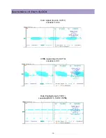
TP564
TP565
TP566
ICS2
TP603
TP604
TP605
PW30
TP159
TP160
JP11
TP161
TP246
PW11
TP162
TP247
TP248
JP12
PW12
TP494 TP508
TP495 TP509
PW7
TP496 TP529
PW15
JP3
PW6
PW21
PW20
P204
TP56
TP63
TP149
TP100
TP57
TP64
P601
TP101
TP58
TP67
TP144
TP102
PW602
TP103
TP143
TP120
TP104
TP121
TP105
TP106
TP107
TP108
TP141
TP109
JP201
JP202
TP27
TP29
TP19
IC201
IC604
IC603
TU1
ICA10
ICV10
JP206
IC601
ICU3
ICD10
ICL10
ICJ10
ICS3
ICS1
ICU10
ICU2
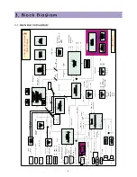
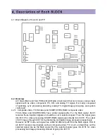
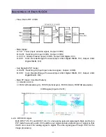
4-1. Block Diagram of main IC and TP
4-2. Overview
A/V block (Main and Sub PCB) is Multi Media circuit board that can process various input
signals such as video, component, PC, DVI, and analog TV signal. It is mainly composed
of switching, sync processing, decoding, analog TV, digital image processing, and system
control part.
4-2-1. Composite video, Y/C(S-Video) and SCART(CVBS, RGB) composite video
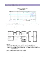
Y/C(S-Video) and SCART(CVBS) have similar signal paths. For the Main signal, IC201
receives these inputted signals and switches out a selected signal. Then the signal goes
into ICV10 for video processing, SCART(RGB) signal goes directly into ICV10. The output
of ICV10 goes through ICS1 for de-interlacing and digital image processing respectively.
However, at PIP mode, sub signal has a little bit different path from the Main signal. First of
all, IC201 receives input signals such as composite video, Y/C or etc, and switches out the
selected signal like as the Main signal. But the selected signal goes into ICS1 for video
processing and image processing instead of going into ICV10.
Summary of Contents for DLP-2612
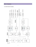
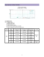
Page 7: ...7 3 2 POWER BLOCK DIAGRAM...
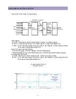
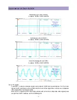
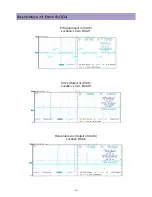
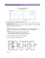
Page 34: ...34 G Signal LCA4 B Signal LCA5 Clock RCA10 near ICA10...
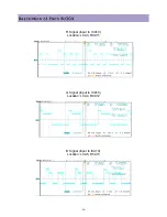
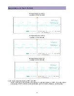
Page 36: ...36 Horizontal sync RCD6 near ICD10 Vertical sync RCD7 near ICD10...
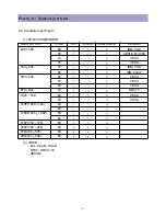
Page 45: ...45 COMPONENT PICTURE REMARK 1 LCD MODULE 2 MAIN BOARD 3 SUB BOARD 4 POWER BOARD...
Page 46: ...46 COMPONENT PICTURE REMARK 5 RONT MASK 6 BACK COVER 7 STAND 8 ALL CONNECTROR CONNECTION...
Page 60: ...11 SCHEMATIC DIAGRAM 62...
Page 61: ...SCHEMATIC DIAGRAM 63...
Page 62: ...SCHEMATIC DIAGRAM 64...
Page 63: ...SCHEMATIC DIAGRAM 65...
Page 64: ...SCHEMATIC DIAGRAM 66...
Page 65: ...SCHEMATIC DIAGRAM 67...
Page 66: ...SCHEMATIC DIAGRAM 68...
Page 67: ...SCHEMATIC DIAGRAM 69...
Page 68: ...SCHEMATIC DIAGRAM 70...
Page 69: ...SCHEMATIC DIAGRAM 71...
Page 70: ...SCHEMATIC DIAGRAM 72...
Page 71: ...SCHEMATIC DIAGRAM 73...
Page 72: ...SCHEMATIC DIAGRAM 74...
Page 73: ...SCHEMATIC DIAGRAM 75...
Page 74: ...SCHEMATIC DIAGRAM 76...
Page 75: ...77 10 1 DLP 3212APSB...
Page 76: ...78 10 2 DLP 2612APSB...


