background image

-3-

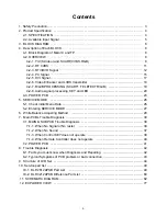
1. Safety Precautions

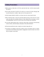
(1) When moving or laying down a LCD Set, please deal with care. Avoid any impact towards

the LCD Set.

(2) Do not leave the broken LCD Set on for a long time. To prevent any further damages, after

check the broken Set

s condition, make sure to turn the power (AC) off.

(3) When opening the BACK COVER, turn off the power (AC) to prevent electric shock. 

(4) When loosening screws, check the connecting position and type of the screw. Sort out the

screws and store them separately. Because screws holding PCB are working as electric

circuit GROUNDING, make sure to check if any screw is missing when assembling.

(5) A LCD Set contain different kind of connector cables. When connecting or disconnecting

connector cables, check the direction and position of the cable beforehand.

(6) When disconnecting connectors, unplug the connectors slowly with care.

(7) Connectors are designed so that if the number of pins or the direction does not match,

connectors will not fit. When having problem in plugging the connectors, make sure to check

their kind, position, and direction.

Summary of Contents for DLP-2612

Page 1: ...oving their performance without notice in the parts list So if you need the latest parts information please refer to PPL Parts Price List in Service Information Center Service Manual LCD TV CHASSIS Mo...

Page 2: ...WER PCB 23 5 SERVICE MODE 26 5 1 Check initial Menu Data 26 5 2 Entering SERVICE MODE 27 6 White Balance Adjusting Method 29 7 Main PCBs Trouble Diagnosis 30 7 1 MAIN SUB PCB Trouble Diagnosis 30 7 1...

Page 3: ...e screw Sort out the screws and store them separately Because screws holding PCB are working as electric circuit GROUNDING make sure to check if any screw is missing when assembling 5 A LCD Set contai...

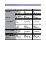
Page 4: ...CAM 2 Carrier NICAM Channel Memory 99ch Auto Preset 99ch Auto Preset INPUT Connector RF 75 Ohm Coaxial 75 Ohm Coaxial S Video 1 1 Scart 2 2 Component RCA 2 RCA 2 PC RGB D Sub 1 D Sub 1 PC Audio 3 5mm...

Page 5: ...PLE MAC66 72 VESA 75 VESA 720 400 70 IBM VGA 85 IBM XGA2 800 600 60 VESA 75 VESA 85 VESA 832 624 74 MAC74 1024 768 60 VESA 70 VESA 720P 1280 720 50 60 1080i 1920 1080 50 60 576P 704 576 50 480P 720 48...

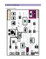
Page 6: ...P RESET SDA 5550M SDA 5550M MICOM MICOM 512K BYTE 512K BYTE FLASHROM FLASHROM CVBS Y C OUT1 CVBS3 Y3 C3 R3 L3 MONITOR CVBS OUT3 L R MAIN L R MONITOR L R MONITOR L R CVBS2 R2 L2 RF CVBS OUT SIF CVBS1 Y...

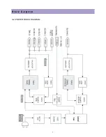
Page 7: ...7 3 2 POWER BLOCK DIAGRAM...

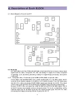
Page 8: ...mposed of switching sync processing decoding analog TV digital image processing and system control part 4 2 1 Composite video Y C S Video and SCART CVBS RGB composite video Y C S Video and SCART CVBS...

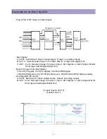
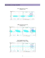
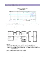
Page 9: ...ital R G B H V Main TP Input Color Bar Pattern CCV15 Y Signal CCV14 C Signal CCV16 CVBS Signal RCS12 Horizontal sync RCS13 Vertical sync RCS14 Clock RCS15 Data enable Sub Signal In PIP mode A IC201 Sw...

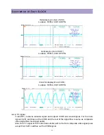
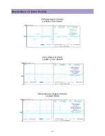
Page 10: ...10 Color signal input to ICV10 Location LCV4 CVBS signal Input to ICV10 Location LCV1 Data Enable Output of ICS1 Loacation RCS15 ICD10 73PIN...

Page 11: ...76PIN 4 2 2 TV signal Tuner TU1 receives antenna signal and outputs CVBS and sound signal For the main signal IC201 switches out the CVBS and the rest of the signal flow is same as composite video sig...

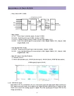
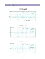
Page 12: ...al Output CVBS B ICS1 Color Decoder Image Processor Input 24bit Digital R G B H V Output 24bit Digital R G B H V Main TP Input Color Bar Pattern CE220 CCV16 RCS12 Horizontal sync RCS13 Vertical sync R...

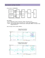
Page 13: ...Location LCA5 RCA14 Main Signal A ICI3 Switching IC Input Component Output Component H V B ICA10 A D converter Input Component H V Output 24bit Digital RGB H V C ICS1 Color Decoder Image Processor In...

Page 14: ...14 Pr Signal Input to ICA10 Location LCA3 RCA11 Clock Output of ICA10 Location LCA1 RCA10 Horizontal sync Output of ICA10 Location RCA9...

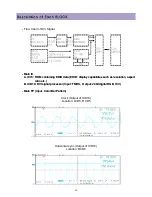
Page 15: ...ignal goes through ICS1 for digital image processing Flow Chart of PC Signal Main IC A ICI3 Switching IC Input Analog RGB H V Output Analog RGB H V B ICA10 A D converter Input Analog RGB H V Output 24...

Page 16: ...16 R Signal Input to ICA10 Location LCA3 RCA11 G Signal Input to ICA10 Location LCA4 RCA12 B Signal Input to ICA10 Location LCA5 RCA14...

Page 17: ...l sync Output of ICA10 Location RCA8 4 2 5 DVI Digital Visual Interface signal To process DVI signal graphic card of AV device reads EDID data from ICI5 ROM Then DVI signal is directly inputted to ICD...

Page 18: ...nput TMDS Output 24bit digital RGB H V Main TP Input Color Bar Pattern Clock Output of ICD10 Location LCD5 RCD5 Horizontal sync Output of ICD10 Location RCD6 Main IC A ICI5 ROM containing EDID data ED...

Page 19: ...er The converted LVDS signal is transmitted to the LCD panel Main IC A ICJ10 Video enhancer Input 24bit digital RGB H V Output 24bit digital RGB H V B ICL10 LVDS transmitter Input 24bit digital RGB H...

Page 20: ...0 Location LCV9 RCV28 B Signal Input to ICV10 Location LCV8 RCV26 4 2 8 Audio signal processing KEY and LED IC201 switches Audio signals and passes a switched signal to IC601 for audio signal processi...

Page 21: ...E618 RC619 Sub L Sound CE617 RC618 Component1 R sound CE616 RC617 Component1 L sound CE615 RC616 Component2 R sound CE614 RC615 Component2 L sound CE613 RC614 PC_L Sound Input to IC201 Location CE208...

Page 22: ...22 IC604 605 INPUT Location L out CE605 R out CE604 Tuner SIF Input Location CC613 TU1 9PIN HEADPHONE Out Location CE636 CE639...

Page 23: ...V Output Voltage and Current are shown below Board Output Minimum output Maximum output Output Current Condition Voltage voltage voltage Continuous 24Vdc 22 8Vdc 25 2Vdc 0 6 0A 5 144Watt 15Vdc 14 25Vd...

Page 24: ...Don t Care OFF 4 3 2 Connectors A AC Connectors P801 I SHENG PLASTIC 7003 7 0MM 3P Power Switch Connector P802 YEON HO YDW236 02P PIN NO CONFIGRATION 1 LIVE Switch PIN1 2 LIVE Switch PIN2 B PL11 PL12...

Page 25: ...ND POWER ON 3 3V POWER ON 4 5V POWER ON 3 3V POWER ON 0V POWER ON 3 3V PIN NO OUT PUT 1 5V 2 5V 3 GND 4 GND 5 6V 6 6V 7 6V 8 GND 9 GND 10 GND D PA12 Pin Spec YEON HO YMW025 10R 10p E PA20 Pin Spec YEO...

Page 26: ...No Super Bass No Equalizer 120Hz 0 500Hz 0 1KHz 0 5KHz 0 10KHz 0 3 Screen Mode 16 9 PC DVI PIP POP Mode No Sub Input TV PIP Size PIP Sound Output Main Color Temp Normal NR On 4 Install Auto tuning Cou...

Page 27: ...LOUR MIN CEN MAX S5 is ON KUMI DEMPOL is selected VOL KEY S5 EEPROM ERASE press menu key then eeprom data is erased excepting factory frequency DECODER SET MAIN SUB Adjustment DEFAULT ADJUSTMENT MAIN...

Page 28: ...PANEL TEST Key Using this key you can test problem of PANEL as confirm white pattern red pattern blue pattern green pattern H S8 8 PANEL WHITE BALANCE Adjustment Key Using this key you can adjust PAN...

Page 29: ...S8 8 Then the set is entered TV WHITE BALANCE Adjustment Mode D Middle BEAM 330 270cd Adjust WHITE BALANCE by varying Gain of R B G fixed Coordinate of color is X 273 5 Y 280 5 And press menu key to c...

Page 30: ...202 Top Sub Negative polarity of CE214 Top Sub near IC201 RC255 Bottom Sub near IC201 CCV16 Top Main near ICV10 If all TP signal does not appear replace SUB PCB Check Star t Does No signal screen appe...

Page 31: ...B PCB 2 Checking waveforms with Color Bar Pattern Using the oscilloscope Main TP Y signal 7th pin of PW202 Top Sub Negative polarity of CE214 Top Sub near IC201 RC10 Bottom Sub near IC201 CCV15 Top Ma...

Page 32: ...JP3 5th pin of ICI2 7th pin of ICI2 14th pin of ICI3 LCA5 Top Main near ICA10 Main TP COMP1_Pr LCI18 Bottom Main near JP3 11th pin of ICI2 9th pin of ICI2 21th pin of ICI3 LCA3 Top Main near ICA10 Mai...

Page 33: ...CA10 Main TP G signal LCI4 Top Main near D Sub Jack 9th pin of ICI3 19th pin of ICI3 LCA4 Top Main near ICA10 Main TP B signal LCI5 Top Main near D Sub Jack 11th pin of ICI3 14th pin of ICI3 LCA5 Top...

Page 34: ...34 G Signal LCA4 B Signal LCA5 Clock RCA10 near ICA10...

Page 35: ...her inputs are working If other inputs are not working replace MAIN or SUB PCB 2 Checking waveforms with Color Bar Pattern Using the oscilloscope Main TP Clock RCD5 Top Main near ICD10 Main TP H Sync...

Page 36: ...36 Horizontal sync RCD6 near ICD10 Vertical sync RCD7 near ICD10...

Page 37: ...Replace SUB PCB IC603 IC604 Problem Replace Sub PCB 1 Check AC connection 2 Check Power S W ON 3 Check Main or other PCBs Check Sound Mute Off Y Y Y Y Y Y N N N N N N Is the Sound input Jack properly...

Page 38: ...ain TP Input to IC601 CE613 COMP2_L CE614 COMP2_R CE615 COMP1_L CE616 COMP1_R CE617 SUB_L CE618 SUB_R CE619 MAIN_L CE620 MAIN_R RC665 MONO CC613 SIF Output to IC601 CE604 R OUT CE605 L OUT 1Khz Sound...

Page 39: ...CON NECTOR 2 Replace KEY PCB Check the connection o f KEY PCB to MAIN PCB Check the connection between KEY PCB and MAIN PCB 1 Check AC co nnection 2 Check Power S W ON 3 Check other PCBs Y Y Y N N N...

Page 40: ...PCB Check the connection between LED PCB and MAIN PCB Check the Battery of Remote Controller 1 Check AC co nnection 2 Check Power S W ON 3 Check other BLOCks When you press button does waveform from...

Page 41: ...Connector 1 Check the Connector 2 Check input Voltage 3 Check PWR CTL PA11 3 4 Check AC DECTED PA11 4 5 Check INV CTI PA11 5 After turn on the power Does LED turn on light After POWER on Does Picture...

Page 42: ...operations explained in this manual include oscilloscope waveforms but these are for reference only and utilizing them to repair PCBs is not necessary F Before replacing PCBs you MUST turn off the AC...

Page 43: ...B B Symptom of No image when LED and Back Light are working Define No image LED and BACK LIGHT of panel are correctly working but any image does not display Repairing method This is typical symptom wh...

Page 44: ...44 1 LCD MODULE 2 MAIN BOARD 3 SUB BOARD HDTV 4 POWER BOARD 5 FRONT MASK 6 BACK COVER 7 STAND 8 ALL CONNECTOR CONNECTION DAEWOO MGDi...

Page 45: ...45 COMPONENT PICTURE REMARK 1 LCD MODULE 2 MAIN BOARD 3 SUB BOARD 4 POWER BOARD...

Page 46: ...46 COMPONENT PICTURE REMARK 5 RONT MASK 6 BACK COVER 7 STAND 8 ALL CONNECTROR CONNECTION...

Page 47: ...CORE FERRITE BNF 2629 ICU3U 149L04070Q IC CHIP FLASH MEMORY F49L040 70NP JP11 4859100780 JACK DVI I AVI 10245 28B JP12 4859203101 CONN D SUB SHF 015 F900 22 NJ JP13 4959101160 JACK STEREO DHAE 9415 J...

Page 48: ...8 CCP9 HCBK104KBA C CHIP CERA 50V X7R 0 1MF K 1608 LOC PARTCODE PARTNAME DESCRIPTION REMARK CCS1 HCQK200JBA C CHIP CERA 50V CH 20PF J 1608 CCS10 HCBK472KBA C CHIP CERA 50V X7R 4700PF K 1608 CCS11 HCQK...

Page 49: ...10 100 OHM J 1608 RCI34 HRFT750JBA R CHIP 1 10 75 OHM J 1608 RCI35 HRFT750JBA R CHIP 1 10 75 OHM J 1608 RCI36 HRFT750JBA R CHIP 1 10 75 OHM J 1608 RCI37 HRFT750JBA R CHIP 1 10 75 OHM J 1608 RCI38 HRF...

Page 50: ...08 CCA8 HCBK104KBA C CHIP CERA 50V X7R 0 1MF K 1608 CCD15 HCBK104KBA C CHIP CERA 50V X7R 0 1MF K 1608 CCD16 HCBK104KBA C CHIP CERA 50V X7R 0 1MF K 1608 CCI11 HCBK103KBA C CHIP CERA 50V X7R 0 01MF K 16...

Page 51: ...CEP9 HCEEF101MC C CHIP ELECTRO MV 16V 100MF 6 3DX5 7H CES10 HCELF220MD C CHIP ELECTRO 16V 22MF CM 4052 CES11 HCELC102ME C CHIP ELECTRO 6 3V 1000MF CM 8010 CES12 HCELC102ME C CHIP ELECTRO 6 3V 1000MF...

Page 52: ...NLC322522 LCP18 HLC479M02D L CHIP COIL 4 7UH M SLF0628 LCP19 HLC109K00C L CHIP COIL 1 0UH K NLC 3225 LCP21 HLC479M02D L CHIP COIL 4 7UH M SLF0628 LCP22 HLC100J00A L CHIP COIL 10UH NLC322522 LOC PARTCO...

Page 53: ...J 1608 RCJ1 HRFT470JBA R CHIP 1 10 47 OHM J 1608 RCJ2 HRFT470JBA R CHIP 1 10 47 OHM J 1608 RCJ3 HRFT470JBA R CHIP 1 10 47 OHM J 1608 LOC PARTCODE PARTNAME DESCRIPTION REMARK RCL10 HRFT000 BA R CHIP 1...

Page 54: ...CERA 50V X7R 0 01MF K 1608 CC204 HCBK103KBA C CHIP CERA 50V X7R 0 01MF K 1608 CC205 HCBK104KBA C CHIP CERA 50V X7R 0 1MF K 1608 CC206 HCBK104KBA C CHIP CERA 50V X7R 0 1MF K 1608 CC207 HCBK104KBA C CHI...

Page 55: ...1608 RC242 HRFT101JBA R CHIP 1 10 100 OHM J 1608 RC243 HRFT101JBA R CHIP 1 10 100 OHM J 1608 LOC PARTCODE PARTNAME DESCRIPTION REMARK RC244 HRFT101JBA R CHIP 1 10 100 OHM J 1608 RC246 HRFT101JBA R CHI...

Page 56: ...0DX5 3H CE615 HCEJK109MC C CHIP ELECTRO MV 50V 1MF 4 0DX5 3H LOC PARTCODE PARTNAME DESCRIPTION REMARK CE616 HCEJK109MC C CHIP ELECTRO MV 50V 1MF 4 0DX5 3H CE617 HCEJK109MC C CHIP ELECTRO MV 50V 1MF 4...

Page 57: ...UH NLC322522 LC611 HLC100J00A L CHIP COIL 10UH NLC322522 LC612 HFF301B00A F CHIP FERRITE BEAD 300 OHM SBK 1608 LC613 HFF301B00A F CHIP FERRITE BEAD 300 OHM SBK 1608 LC614 HFF301B00A F CHIP FERRITE BEA...

Page 58: ...FZN PTSBMSG099 7178301011 M492A SCREW TAPPTITE TT2 WAS 3X10 MFZN PTCACAG099 4856013600 M492A SCREW SPKR FIX SWRM SECC PTCACAG098 7173301012 M722A SCREW TAPTITE TT2 BIN 3X10 MFZN BK PTCACAG098 PTCACAG0...

Page 59: ...AS DLP 3212APSB PTMPJ0G099 PTMPJRG099 ZZ200 PCB MAIN RADIAL AS DLP 3212APSB PTMPJBG099 PTSBJ0G099 ZZ200 PCB SUB RHU AS DLP 3212APSB PTSBJ2G099 PTSBJ1G099 ZZ200 PCB SUB CHIP A AS DLP 3212APSB PTSBJAG09...

Page 60: ...11 SCHEMATIC DIAGRAM 62...

Page 61: ...SCHEMATIC DIAGRAM 63...

Page 62: ...SCHEMATIC DIAGRAM 64...

Page 63: ...SCHEMATIC DIAGRAM 65...

Page 64: ...SCHEMATIC DIAGRAM 66...

Page 65: ...SCHEMATIC DIAGRAM 67...

Page 66: ...SCHEMATIC DIAGRAM 68...

Page 67: ...SCHEMATIC DIAGRAM 69...

Page 68: ...SCHEMATIC DIAGRAM 70...

Page 69: ...SCHEMATIC DIAGRAM 71...

Page 70: ...SCHEMATIC DIAGRAM 72...

Page 71: ...SCHEMATIC DIAGRAM 73...

Page 72: ...SCHEMATIC DIAGRAM 74...

Page 73: ...SCHEMATIC DIAGRAM 75...

Page 74: ...SCHEMATIC DIAGRAM 76...

Page 75: ...77 10 1 DLP 3212APSB...

Page 76: ...78 10 2 DLP 2612APSB...

Page 77: ...DAEWOO ELECTRONICS CORP PRINTED DATE NOV 2005 686 AHYEON DONG MAPO GU SEOUL KOREA C P O BOX 8003 SEOUL KOREA...

Reviews: