- 37 -
Service manual WP 895/895F, CP885/885F
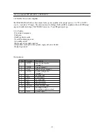
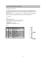
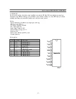
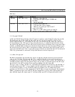
4-6 24C16 - 16 Kb EEPROM
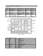
features :
- 16 Kbit serial I2C bus EEPROM
- Single supply voltage : 4.5 V to 5.5 V
- 1 Million Erase/Write cycles (minimum)
- 40 year data retention (minimum)
Pin description
Pin No.
Name
Description
1, 2, 3
E0, E1, E2
Device address - not used
5
SDA
Serral Data/Address Input/Output
6
SCL
Serial clock
7
WC
Write control
8
Vcc
Supply voltage
4
Vss
Ground
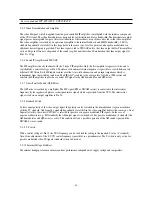
The memory device is compatible with the I2C memory standard. This is a two wire serial interface that uses a
bi-directionnal data bus and serial clock. The memory carries a built-in 4-bit unique device type identifier code (1010)
in accordance with the I2C bus definition.
Serial Clock (SCL)
The SCL input is used to strobe all data in and out of the memory.
Serial Data (SDA)
The SDA pin is bi-directionnal, and is used to transfer data in or out of the memory
Summary of Contents for CP-885
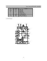
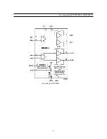
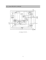
Page 32: ... 31 Service manual WP 895 895F CP885 885F Block diagram TDA8944J ...
Page 35: ... 34 Service manual WP 895 895F CP885 885F ...
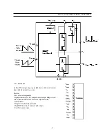
Page 37: ... 36 Service manual WP 895 895F CP885 885F Block diagram TDA6107Q ...
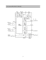
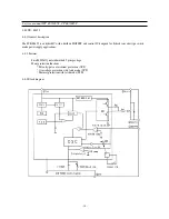
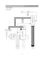
Page 42: ... 41 Service manual WP 895 895F CP885 885F 5 Circuit description 5 1 Block diagram ...
Page 60: ... 59 Service manual WP 895 895F CP885 885F 5 9 2 2 STR F6654 oscillating operation ...
Page 76: ...Service Manual WP 895 895F CP885 885F 75 7 Exploded View 7 1 DWX 28W5 ...
Page 77: ...Service Manual WP 895 895F CP885 885F 76 7 Exploded View 7 2 DWF 28W8 ...
Page 78: ...Service Manual WP 895 895F CP885 885F 77 7 Exploded View 7 3 DTF 29U8 ...
Page 79: ...Service Manual WP 895 895F CP885 885F 78 7 Exploded View 7 4 DTP 28A7 ...
Page 80: ...Service Man ual WP 895 895F CP885 885F 79 7 Exploded View 7 5 DTP 28B1 ...
Page 81: ...Service Man ual WP 895 895F CP885 885F 80 7 Exploded View 7 6 DTP 28G7 ...
Page 82: ...Service Manual WP 895 895F CP885 885F 81 7 Exploded View 7 7 DTP 28G8 ...
Page 83: ...PRINTED CIRCUIT BOARD PCB MAIN ...
Page 84: ......
Page 85: ......

