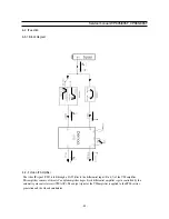
- 28 -
Service manual WP 895/895F, CP885/885F
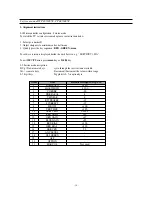
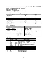
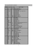
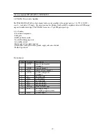
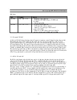
Pin No.
Pin Name
Type
Short description
59
ANA_IN1-
In
IF common
60
NC
Not Connected
61
TESTEN
In
Test pin
62
XTAL_IN
In
Crystal oscillator
63
XTAL_OUT
Out
Crystal oscillator
64
NC
Test pin
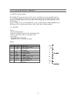
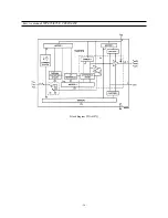
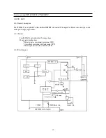
4-3 TDA 4470-Multistandard Video-IF and Quasi Parallel Sound Processor
4-3-1- Description
The TDA 4470 is an integrated bipolar circuit for multi-standard video/sound IF (VIF/SIF) signal processing in
TV/VCR and multimedia applications. The circuit processes all TV video IF signals with negative modulation
(e.g., B/G standard), positive modulation (e.g., L standard) and the AM, FM/NICAM sound IF signals.
4-3-2- Features
- 5V supply voltage ; low power consumption.
- Active carrier generation by FPLL principle (frequency-phase-locked-loop) for true synchronous demodulation.
- Very linear video demodulation, good pulse response and excellent intermodulation figures.
- Alignment-free AFC without external reference circuit, polarity of the AFC curve is switchable.
- VIF-AGC for negative modulated signals (peak sync. detection) and for positive modulation
(peak white/black level detector).
- Tuner AGC with adjustable take over point.
- Alignment-free quasi parallel sound (QPS) mixer for FM/NICAM sound IF signals.
- Intercarrier output signal is gain controlled (necessary for digital sound processing).
- Complete alignment-free AM demodulator with gain controlled AF output.
- Separate SIF-AGC with average detection
- Two independent SIF inputs
- Parallel operation of the AM demodulator and QPS mixer (for NICAM-L stereo sound).
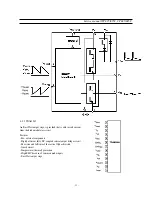
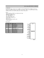
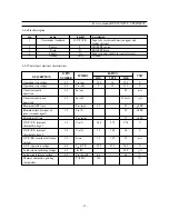
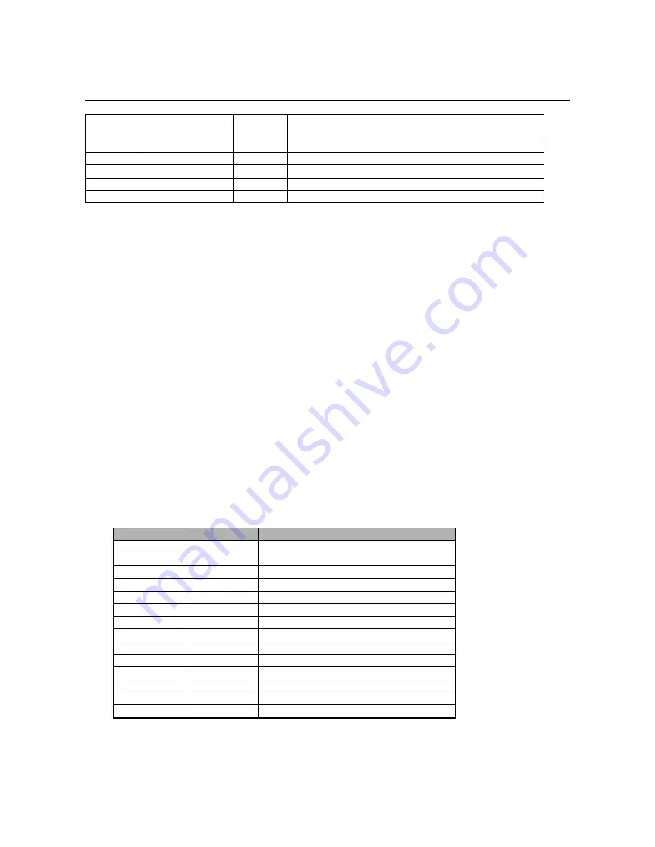
4-3-3- Pinning
Pin
Symbol
Function
1,2
V
i,SIF1
SIF1 input ( symmetrical)
3
V
SW
Input selector switch
4,9,16
GND
Ground
5
V
AGC
SIF-AGC (time constant)
6,7
V
i,VIF
VIF input (symmetrical)
8
C
AGC
VIF-AGC (time constant)
10
R
TOP
Take Over Point, tuner AGC
11
I
tun
Tuner AGC output current
12
V
O,VID
Video output
13
V
SW
Standard switch
14
V
SW
L’switch
15
C
bl
Black level capacitor
17
C
ref
Internal reference voltage
18
LF
Loop Filter
Summary of Contents for CP-885
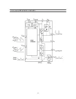
Page 32: ... 31 Service manual WP 895 895F CP885 885F Block diagram TDA8944J ...
Page 35: ... 34 Service manual WP 895 895F CP885 885F ...
Page 37: ... 36 Service manual WP 895 895F CP885 885F Block diagram TDA6107Q ...
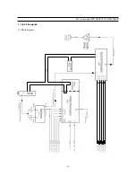
Page 42: ... 41 Service manual WP 895 895F CP885 885F 5 Circuit description 5 1 Block diagram ...
Page 60: ... 59 Service manual WP 895 895F CP885 885F 5 9 2 2 STR F6654 oscillating operation ...
Page 76: ...Service Manual WP 895 895F CP885 885F 75 7 Exploded View 7 1 DWX 28W5 ...
Page 77: ...Service Manual WP 895 895F CP885 885F 76 7 Exploded View 7 2 DWF 28W8 ...
Page 78: ...Service Manual WP 895 895F CP885 885F 77 7 Exploded View 7 3 DTF 29U8 ...
Page 79: ...Service Manual WP 895 895F CP885 885F 78 7 Exploded View 7 4 DTP 28A7 ...
Page 80: ...Service Man ual WP 895 895F CP885 885F 79 7 Exploded View 7 5 DTP 28B1 ...
Page 81: ...Service Man ual WP 895 895F CP885 885F 80 7 Exploded View 7 6 DTP 28G7 ...
Page 82: ...Service Manual WP 895 895F CP885 885F 81 7 Exploded View 7 7 DTP 28G8 ...
Page 83: ...PRINTED CIRCUIT BOARD PCB MAIN ...
Page 84: ......
Page 85: ......

