CY8CKIT-147 PSoC® 4100PS Prototyping Kit Guide, Doc. #: 002-18734 Rev. *D
19
3.
Kit Operation
This chapter introduces you to the different features of the PSoC 4100PS Prototyping kit. This pri-
marily includes the programming/debugging functionality, KitProg2 USB-UART and USB-I2C
bridges, and the method to update the KitProg2 firmware.
3.1
Theory of Operation
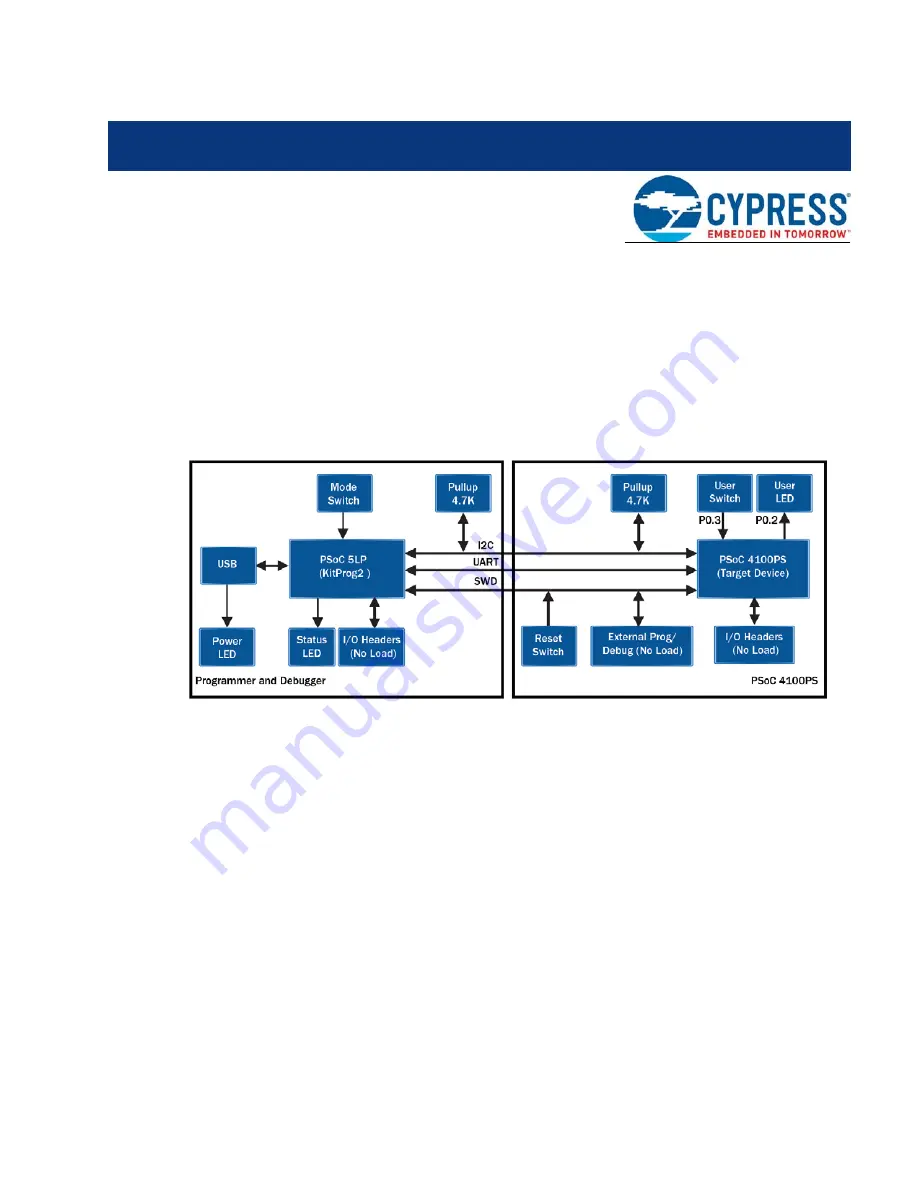
shows the block diagram for the PSoC 4100PS Prototyping kit.
Figure 3-1. Block Diagram of PSoC 4100PS Prototyping kit
The PSoC 4100PS Prototyping kit is simplistic in design and focuses on providing you with complete
access to develop applications using the PSoC 4100PS device family. This kit supports the following
features:
■
PSoC 4100PS I/O Headers:
The PSoC 4100PS Prototyping board brings all GPIOs of the target
PSoC 4100PS device to the two expansion headers, enabling the user to have maximum access
to the capabilities of the PSoC 4100PS device.
■
User LED:
The on-board LED can be used to display outputs from the PSoC 4100PS device.
This includes modulating the brightness of the LED to notify different states of the device.
■
User Button:
This kit has a push button, which can be used to provide an input to the
PSoC 4100PS.
Note:
The switch connects the PSoC 4100PS pin to ground when pressed. Therefore, you need
to configure the PSoC 4100PS pin as ‘resistive pull-up’ for detecting the switch press. Also note
when configuring the pin as ‘resistive pull-up’, the pin cannot be connected to any other internal
peripheral through hardware connection.


