CY8CKIT-147 PSoC® 4100PS Prototyping Kit Guide, Doc. #: 002-18734 Rev. *D
42
A.3
PSoC 4100PS Prototyping kit Schematics
Refer to the schematic file in the following path in the installed kit software:
<Install_Directory>\CY8CKIT-147 PSoC 4100PS Prototyping Kit\
<version>\Hardware\CY8CKIT-147 Schematic.pdf
A.4
Bill of Materials
Refer to the BOM file in the following path in the kit software installed:
<Install_Directory>\CY8CKIT-147 PSoC 4100PS Prototyping Kit\
<version>\Hardware\CY8CKIT-147 PCBA_BOM.xlsm
A.5
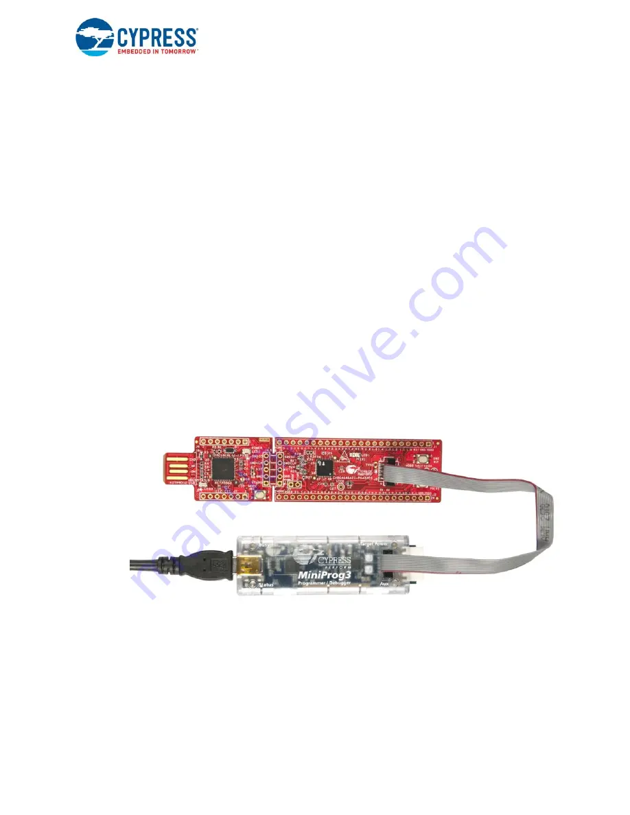
Programming PSoC 4100PS Prototyping kit Using MiniProg3/
KitProg2
The target board provides a provision to program the PSoC 4100PS device using MiniProg3 or an
external KitProg2 via the 10-pin JTAG header or the 5-pin SWD header. To do this, connect wires or
a 5-pin 100-mil spaced header to J5 or a 10-pin JTAG header to J9 on the target board. The
PSoC 4100PS Prototyping kit supports both power cycle and reset programming modes. The 10-pin
header can also be used to connect a third party debugger.
Figure A-16. Connecting the CY8CKIT-147 to a MiniProg3
Note:
is not part of the PSoC 4100PS Prototyping Kit contents and can be
.


