background image

Chapter 6: Instructions

119

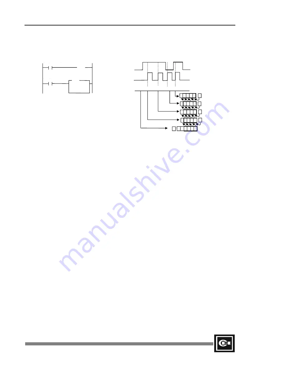
Example

Program Expression

Operation Results


If N = 1, the bits shift by one, and the LSB is always
input from F1.8.


If N = 2, the bits shift by two. The bits are shifted one
position, and the first data input to the LSB is F1.8.
The original MSB is stored in F1.8. The bits are
again shifted one position, with the LSB being set by
the new F1.8, and F1.8 being changed to the state of
the last MSB.

  R0.0

    R

  R0.1
    R

ROL
D =MO
N = 1

F1.8
(OUT)

      M0     $00   $01       $03         $06  $0D
   (word)
                                                                      … 1  1  0  1     1   C

                                                                      … 0  1   1  0    0   C

                                                                      …  0  0  1  1     1  C

                                                                       … 0  0  0  1     1  C

                                                        C  0    0  …  0  0  0  0

R0.0

R0.1

Summary of Contents for D320 PLC

Page 1: ...D320 PLC User s Manual...

Page 2: ...ans electronic mechanical photocopying recording or otherwise without prior written permission of Cutler Hammer Inc RESTRICTED RIGHTS LEGEND Use duplication or disclosure by the Government is subject...

Page 3: ...Preface i Preface Welcome to Cutler Hammer s D320 PLC User s Manual This preface describes the contents of this manual and provides information on Support Services...

Page 4: ...e Chapter 1 Introduction Chapter 2 System Configuration Chapter 3 Product Specification Chapter 4 Installation and Wiring Chapter 5 CPU Operation and Memory Chapter 6 Instructions Chapter 7 Testing an...

Page 5: ...ot currently include product repairs or shipping outside normal business hours Technical Support Fax 614 882 0417 You can also contact our technical support engineers by faxing your support requests d...

Page 6: ...2 x7601 or fax 614 882 3414 Product Ordering Service 614 882 3282 FAX 614 882 6532 Authorized Cutler Hammer distributors may place product orders directly with our Order Processing department by calli...

Page 7: ...er 2 System Configuration 7 D320 PLC System Components 8 D320 PLC Product List 9 D320 PLC I O Configuration 14 Module Placement Requirements 14 D320 PLC Backplane Configurations 15 Chapter 3 Product S...

Page 8: ...ode operating 47 Stop Mode 47 Remote Mode 47 Error Mode 47 CPU Processing Procedure 48 Program Processing Procedure 48 Introduction to Registers 49 Internal External Address Designation 50 Expression...

Page 9: ...EC DECB DDECB 101 Arithmetic Instruction Details 102 ADD DADD ADDB DADDB 102 SUB DSUB SUBB DSUBB 104 MUL DMUL MULB DMULB 105 DIV DDIV DIVB DDIVB 106 ADC DADC ADCB DADCB 107 SBC DSBC SBCB DSBCB 109 ABS...

Page 10: ...es 168 Correcting Errors 170 System Check 170 Power Supply Check 171 Run Check 172 Error Check 173 I O Check 174 External Environment Check 176 Troubleshooting Maintenance and Inspection Tables 177 Pe...

Page 11: ...2 Query Acknowledge QA 200 Step 3 Response Request RR 200 Step 4 Response R 200 Step 5 Repeated Response 201 Communications Delay 201 Example 201 CPU ID 202 Function Codes Included in the Query 202 C...

Page 12: ...s Manual Description of Operation MODBUS RTU mode 235 MODBUS Memory Mapping 235 Description of Operation UDCP Mode 236 Example 1 Printing an Error Message from an Input 237 Example 2 D320 Master on D...

Page 13: ...esigned to handle a wide range of application This manual will give you a complete understanding of how to install and program the D320 PLC It also includes complete product specifications and a descr...

Page 14: ...dures for D320 PLC communication Appendix B details the configuration and operation of PID Loop Control on the D320 PLC Appendix C describes the enhanced operation of the CPU s second program loader p...

Page 15: ...on control Real time Clock A real time clock RTC function enables time and date related programming tasks including alarm recording process scheduling and product serialization Large Program Memory Su...

Page 16: ...can be used System Installation Considerations Environmental Considerations The D320 PLC system should never be installed under the following environmental conditions 1 Ambient temperature outside th...

Page 17: ...ate the main PLC power line ground from all other power grounds Always use triple grounding 3 Do not exceed the current and power rating of the external 24 VDC provided by the D320 power supply 4 Avoi...

Page 18: ...6 D320 PLC User s Manual...

Page 19: ...ailable for the D320 PLC It includes a diagram that shows the D320 PLC system components I O configurations and backplane configurations This chapter contains Information about the D320 PLC system com...

Page 20: ...ule W LINK Module Remote I O Slave Module CPU Module Power Module AC DC Remote I O Master Module Analog A D D A RTD T C HSC Module 16 32p Digital I O Module Base backplane 3 5 8 slot Expansion backpla...

Page 21: ...munications ports Backplanes Name Catalog Product Description Remarks D320RAK03B 3 slot type D320RAK05B 5 slot type Base Backplane D320RAK08B 8 slot type D320RAK05E 5 slot type Expansion Backplane D32...

Page 22: ...Y output 250 V 3 A 8 points 5 A common D320DOM1600V RELAY output 250 V 3 A 8 points 5 A common varistor protection D320DOM1624D TR output NPN 12 to 24 VDC 0 6 A 8 points 4 A common 16 point D320DOM161...

Page 23: ...Analog Output 4 Ch D320AOM420C 4 Ch current output 14 bit D A converter 4 to 20 mA Conversion speed 2 5 ms Ch Resolution 4 A 1 bit RTD Input D320RTD800 8 Ch 24 bit A D converter 3 wire 0 1 C Pt 100 J...

Page 24: ...Remarks Remote I O Master Module D320RMU300 Master Unit installed on main rack with CPU Remote I O Slave Module D320RSU300 Replaces CPU on remote backplanes D320RIM1624D 16 points DC IN terminal type...

Page 25: ...shooting and diagnostic features For Windows 3 1 95 98 NT Note When this manual uses the term GPC either GPC5 or WinGPC can be used Programming Cables Name Catalog Product Description Remarks RS232C 4...

Page 26: ...nstallation Base System Power Supply Slot to extreme left CPU Module Second slot from left I O Module Any slot to right of CPU Serial Data Unit SDU Any slot to right of CPU Remote I O Slave Install in...

Page 27: ...o different slot types 5 slot and 8 slot A maximum of three expansion backplanes can be installed in addition to the base backplane A maximum of 1 024 local control points are available This is achiev...

Page 28: ...16 D320 PLC User s Manual...

Page 29: ...vironmental conditions for D320 PLC operation and the performance specifications and component functions of the CPU This chapter discusses The environmental operating ranges for the D320 Series produc...

Page 30: ...and earth AC 1500 V for 1 min Breakdown voltage Between DC external terminal and earth AC 500 V for 1 min Insulation resistance Between AC external terminal and earth AC 1500 V for 1 min Vibration re...

Page 31: ...M063 15 1 024 points 64 words loop 1 Internal contact M M000 0 to M127 15 2 048 points 128 words Retentive internal contact K K000 0 to K127 15 2 048 points 128 words System flags F F000 0 to F015 15...

Page 32: ...play LEDs provide the following information LED Color Function RUN Green On when CPU is in Run mode PROG Green On when program is in Stop Program mode TEST Green On when CPU is in Test mode ERROR Red...

Page 33: ...d Off Off Terminating resistors for RS485 communications not connected 5 6 On On Terminating resistors for RS485 communications connected CAUTION The communication port can be used for an RS232 or RS4...

Page 34: ...22 D320 PLC User s Manual...

Page 35: ...ter provides considerations and information on installing and wiring the D320 PLC Diagrams are included to illustrate the installation procedures This chapter contains System design considerations Sys...

Page 36: ...The potentially dangerous effects of these errors on the whole system can be prevented with proper safety precautions The use of properly designed safety circuits external to the PLC will protect aga...

Page 37: ...operation depends on circumstances at that time and is not defined The control system should be designed specifically to ensure safe operation for these potential power loss conditions Voltage Drop B...

Page 38: ...ontrol Panel Installation Leave enough space at the top of unit from other devices or wiring ducts to allow ventilation space and easy replacement and wiring of the unit see the following diagrams Do...

Page 39: ...optical link module Leave 4 inches 100 mm or more for the wire link module This allows for extra ventilation space and reduces noise interference When installing the PLC in a cabinet or enclosure Leav...

Page 40: ...Number Size A in mm Size B in mm 3 D320RAK03B 10 25 260 9 65 254 5 D320RAK05B 13 0 330 12 4 315 Base Backplane 8 D320RAK08B 17 15 435 16 55 420 5 D320RAK05E 13 0 330 12 4 315 Expansion Backplane 8 D32...

Page 41: ...e flanges at the base of the module into the slots at the bottom of the I O backplane 2 Swing the I O module up onto the backplane pressing firmly onto the backplane connector 3 Tighten the screw at t...

Page 42: ...m Expansion Cable Connection Connecting the Expansion Cable The expansion cable is connected between the connectors marked IN and OUT on the backplane The expansion cable should not be run in the same...

Page 43: ...power cable To reduce power loss in the wiring use at least 14 AWG 2 mm cable To reduce the effect of noise use twisted shielded cable An isolation transformer can be used to further reduce noise and...

Page 44: ...FG terminals must be kept separate to prevent ground loops in the power supply system 120 240 VAC Power Supply Wiring Diagram Right Wrong PLC Other device Other device PLC If the noise effect is large...

Page 45: ...sed The input device connection methods are shown in the following graphics for the various types of digital input devices DC Sensor The following diagrams show the input device in connection with a D...

Page 46: ...pe DC Load Sensor I n t e r n a l C i r c u i t VCC Sensor Output Input Termina l COM 0 V Input Power Module Sensor I n t e r n a l C i r c u i t Input Terminal COM Terminal Input Power Sensor Module...

Page 47: ...20DIM1624D 12 to 24 VDC type input module Off voltage 2 5 V input impedance 3 k If the Off voltage of the input is 2 5 V set R so that the voltage between the input terminal is below 2 5 V Input imped...

Page 48: ...urrent I can be directly calculated in the following equation the Off voltage of the input is 2 5 V and power voltage is 24 V I 24 2 5 r Alternatively the value of I can be experimentally calculated b...

Page 49: ...e the output modules only within the specified ranges of operation Inductive Loads For an inductive load connect the protective circuit in parallel with the load When opening or closing a DC inductive...

Page 50: ...before the internal fuse blows Be certain to provide the proper level of short circuit protection for a given output type Leakage Current When using an SSR output to a load that draws a very low level...

Page 51: ...le terminal strips on the I O modules for the D320 PLC use an M3 5 metric screw Either open or circular type connectors may be used for attaching the control wiring to the terminal strip Removing Term...

Page 52: ...for connection to the I O module and 20 separate open type screw connectors at the other for connecting the field devices The cable is 5 feet in length Product Name Product Code Product Specification...

Page 53: ...R0 12 R0 12 R0 12 I 14 R0 13 R0 13 R0 13 I 15 R0 14 R0 14 R0 14 I 16 R0 15 R0 15 R0 15 I 17 COM1 COM I 18 COM1 COM I 19 COM2 COM 24VDC I 20 COM2 COM 24VDC Connector II I O Point D320DIM3224D D320DOM32...

Page 54: ...tacts are provided for use as either an external alarm indication for system fault or for wiring as part of the emergency stop circuit for the system They provide a PLC independent method of indicatio...

Page 55: ...M1 9600 19200 COM2 9600 19200 38400 Protocol Half duplex asynchronous polling Parity No parity Stop bit 1 Stop bit Cable type Twisted pair cable Use Shielded cable Program Loaders D320PGM500 GPC5 WinG...

Page 56: ...2 m RS232C shared cable wiring diagram D320CBL50 15 feet 5 m IBM PC computer 25 pin female PLC 9 pin male D320CBL50 2 3 4 5 6 7 20 2 3 4 5 6 7 D320CBL20 IBM PC computer PLC 9 Pin D sub cable female 9...

Page 57: ...h information about memory addresses and the CPU operation It includes a terminology section and an overview of registers This chapter discusses The terminology used in the D320 PLC manual CPU operati...

Page 58: ...ical PLC application most of the scan time is used to process the program When programming keep in mind that the scan time will increase as you increase the number of inputs and outputs and or the siz...

Page 59: ...he external outputs are updated every scan according to program results Stop Mode The user program is stopped and the external outputs are turned Off In the Stop mode you can correct delete and transf...

Page 60: ...CPU Processing Procedure Program Processing Procedure The diagram indicates the PLC program processing procedure The CPU regularly repeats procedure 1 through 5 This cycle is called 1 scan time 1 Man...

Page 61: ...e 2 M Memory register Can be bit word or double word An internal bit memory address which supports relay logic operations Can also be used as a word or double word variable for general calculations an...

Page 62: ...n referenced as SV000 to SV255 5 The Present Value of timers and counters is stored above the Set Values in the W registers from W2304 to W2559 These values can also be addressed using the PV designat...

Page 63: ...Set Value PV is Present Value SV can hold values from 0 to 65535 Data Word W0000 to W2047 Word value memory area Used for tables data storage and math operations Cannot be designated with a bit Syste...

Page 64: ...ction are double word instructions and process the data as 32 bit double words Example 1 Example 2 Example 3 Comparison Instruction Word Double word W0 is processed as 16 bit 1 word data 0 to 65 535 S...

Page 65: ...L0063 191 00BF Data Area W2047 2559 09FF M0000 192 00C0 W2048 2560 0A00 M0001 192 00C1 W2049 2561 0A01 M0002 194 00C2 M0003 195 00C3 T C Set Value W2303 2815 0AFF W2304 2816 0B00 M0126 318 013E W2305...

Page 66: ...ss 0 The CPU automatically determines whether the register data from the modules is of type input or output The 16 point I O modules use one word of register memory The 32 point I O modules require 2...

Page 67: ...ting station information Loop 1 F6 register Link status flag Link data receiving information flag Loop 0 F7 register Link status flag Link data receiving information flag Loop 1 F8 register Remote con...

Page 68: ...the CPU keeps running Turned off when the error is corrected Normal Off F0 7 Module type error On when module information that is stored in the CPU and module that is installed are different types Th...

Page 69: ...error display On when the K retentive data is destroyed and or changed F1 8 Carry Flag On in the event of carry when performing math instructions ADD SUB etc F1 9 Division by zero error On when the d...

Page 70: ...8 bits 0 to 223 are the valid user defined values 255 is the default value SR001 CPU status Indicates current CPU information state stop remote control mode run mode error Error 1 Run control same as...

Page 71: ...n Stores high order 8 bit values upon executing 16 bit multiplication instructions SR022 Remainder Stores the remainder after a division instruction has been executed high order 16 bits SR024 to 27 Re...

Page 72: ...PR OUTR is beyond the specified range or if it designates a module which is not installed 4 On if an undefined instruction exists 5 On in the event of a user program memory error 6 On in the event of...

Page 73: ...h SR296 Second 00 Set Time SR297 Hour minute bit 0 bit change Note 1 Set the range as follows Year 00 to 99 Month 01 to 12 Date 01 to 31 Day 01 to 07 Sun to Sat Hour 00 to 23 Minute 00 to 59 Second 00...

Page 74: ...ng WinGPC as follows Go online with the D320 by clicking on the Online button on the toolbar or by selecting Online from the Online menu Enter the PLC ID or 255 for direct connection and password and...

Page 75: ...2064 W2320 56 W2104 W2360 96 W2144 W2400 17 W2065 W2321 57 W2105 W2361 97 W2145 W2401 18 W2066 W2322 58 W2106 W2362 98 W2146 W2402 19 W2067 W2323 59 W2107 W2363 99 W2147 W2403 20 W2068 W2324 60 W2108...

Page 76: ...9 231 W2279 W2535 140 W2188 W2444 186 W2234 W2490 232 W2280 W2536 141 W2189 W2445 187 W2235 W2491 233 W2281 W2537 142 W2190 W2446 188 W2236 W2492 234 W2282 W2538 143 W2191 W2447 189 W2237 W2493 235 W2...

Page 77: ...psed time and the counter number of counts Note When using GPC software the above W registers can be represented as follows Ch Set Value SV Present Value PV 0 W2048 SV0 W2304 PV0 1 W2049 SV1 W2305 PV1...

Page 78: ...66 D320 PLC User s Manual...

Page 79: ...that are used with the D320 PLC The instructions are grouped by function and then explained in detail This chapter discusses The instructions that are used with the D320 PLC How to read the descriptio...

Page 80: ...T Not Invert logic result STR DIF Start Differential R Start rising edge contact STR DFN Start Dif Not F Start falling edge contact AND DIF And Dif R Rising edge series connection AND DFN And Dif Not...

Page 81: ...3 SV 5 R Up counter input output reset present value set value Range of channel Ch 0 to 255 Shared with timer Setting range SV 0 65535 Done Contact TC channel no DC Down Counter DC U CH 14 SV 5 R Down...

Page 82: ...than B D value Substitution Increment Decrement Instructions Note Application instructions that operate on double words 32 bit are designated with a D in front of the single word instruction For exam...

Page 83: ...tiplication MULB D S1 S2 DMULB D S1 S2 D S1 S2 BCD operation DIVB DDIVB BCD division DIVB D S1 S2 DDIVB D S1 S2 D S1 S2 BCD operation ADC DADC Decimal addition w carry ADC D S1 S2 DADC D S1 S2 D S1 S2...

Page 84: ...e Word Description RLC DRLC Rotate left without carry RLC D N DRLC D N Rotate contents of designated register D to the left N times lower higher F1 8 15 D 0 RRC DRRC Rotate right without carry RRC D N...

Page 85: ...0 0 0 0 1 0 1 D 0 1 1 0 1 1 0 1 g f e d c b a 5 a f b g e c d ENCO Encode ENCO D S Store the location of the highest set bit in S in D 15 8 7 6 5 4 3 2 1 0 S 0 0 0 1 1 1 0 0 0 0 D 0 0 0 0 0 1 1 1 6 1...

Page 86: ...D N Reverse state of Nth bit of D D 0 1 1 1 0 1 0 0 N 4 D 0 1 1 0 0 1 0 0 BTST Bit Test BTST D N Set carry bit F1 8 to the state of the Nth bit of D D 0 1 1 1 0 1 0 0 N 6 F1 8 SUM Sum SUM D S Store t...

Page 87: ...words from Sr to D Sr 1 0 1 0 1 0 1 0 Sr 1 0 0 0 0 1 1 1 1 Sr 2 1 1 1 1 0 0 0 0 Ns 3 D 1 0 1 0 1 0 1 0 D 1 0 0 0 0 1 1 1 1 D 2 1 1 1 1 0 0 0 0 FMOV Fill Move FMOV D Ns V Repeatedly copy the value V Ns...

Page 88: ...L Label LBL L Position jumped to by JMP instruction L 0 to 63 JMPS Jump Start JMPS Jump to JMPE instruction JMPE Jump End JMPE Position jumped to by JMPS instruction CALL Call Subroutine CALL Sb Call...

Page 89: ...D To NR1 RR2 Nt NN3 NN4 Fr NN5 NR6 Read NR1 words from remote I O loop NN3 station NN4 slot NN5 module memory address NR6 and store in words starting at RR2 RMWR Write data remote I O intelligent I O...

Page 90: ...odes unavailable option available option xx indicates a hexadecimal number Explanation of Table Mnemonic A word instruction D designates double word instruction Assignment expression Description of th...

Page 91: ...on is true Explanation of Description The description provides details of the instruction Sample Example Program Expression Time Chart Explanation of Example The example shows an application of an ins...

Page 92: ...the ladder program begins with either a STR or STN 2 Every rung will contain one or more contacts 3 Every rung will end in one or more output coils or application instructions 4 When programming a la...

Page 93: ...OT indicate a series connection of each contact 2 The number of ANDs and ADNs used within one branch rung is unlimited 3 M100 15 is On only when contact R000 3 is On and contact R000 4 is Off M100 15...

Page 94: ...l connection ORN NC normally closed contact parallel connection Description 1 OR and ORN OR NOT indicate parallel connection of each contact 2 The number of ORs and ORNs used within a branch is unlimi...

Page 95: ...and retentive K contacts The same address can be used more than once When the input conditions are true the coil is turned On and stays on unless turned off by a RST The output is turned Off in the St...

Page 96: ...s of the NOT execution Before After A On B Off A Off B On Description 1 The instruction cannot be connected directly to the bus it must come after a contact or set of contacts 2 The instruction direct...

Page 97: ...e DIF instruction is a contact which is On for the first scan after the signal has changed from Off On The contact is Off for all other scans when the signal has not changed from Off or On 3 The DFN i...

Page 98: ...2 Block in parallel Parallel connection of more than two contacts Starts with STR or STN Ends with ORB 3 When programming in ladder GPC will automatically add the proper ANB and ORB instructions as re...

Page 99: ...When the input conditions to the MCS are false the block of instructions that follow are executed as false Must be used with MCR 2 MCR Master Control Reset Marks the end of a conditional block of inst...

Page 100: ...output is Off Valid channel numbers Ch 0 through Ch 255 256 channels Done contact TC channel number Description 1 Ch 0 to Ch 63 Time base 0 01 sec 10 msec Ch 64 to Ch 255 Time base 0 1 sec 100 msec 2...

Page 101: ...Chapter 6 Instructions 89 Example Program Expression Time Chart R000 0 0 7 sec TC25 R000 1 7 sec TC200 R000 0 R000 1 TC025 TC200 TIM T CH 25 SV 70 SST T CH 200 SV 70 M11 5 OUT M22 5 OUT...

Page 102: ...T instruction in which the PV counts up from 0 the timer elapsed value PV decreases from SV when the input is turned Off until it reaches 0 If the input is turned On again before the output turns Off...

Page 103: ...e PV is set to 0 Description 1 The timer counter channel can only be used once It cannot be reused by other timer or counter instructions TIM SST TOF RCT UDC A maximum of 256 channels Ch 0 to Ch 255 c...

Page 104: ...92 D320 PLC User s Manual Example Program Expression Time Chart R000 0 UC U CH 0 R000 1 SV 3 R TC000 M0 0 OUT R000 0 R000 1 counter time value 0 1 2 3 4 0 0 1 Output TCO...

Page 105: ...nput pulses are ignored and the Present Value stays reset to 0 3 When the SV of the counter is 0 the output done contact is On unless the reset input is On 4 The timer counter channel can only be used...

Page 106: ...down count input pulse occur at the same time the PV does not change 5 When the PV is 0 if the down count pulse is input the Present Value does not change and the output is On When the Present Value i...

Page 107: ...ructions 95 Example Program Expression Time Chart U input R0 0 Down Input R0 1 Reset Input TC15 Present Value PV64 0 1 2 3 4 5 4 3 2 1 0 0 1 2 3 4 0 Output TC64 R000 0 UDC U CH 64 R000 1 SV 3 S TC15 R...

Page 108: ...Shift Pulse input P input is turned on the starting contact Sb is set to the state of the Input Data input I input 4 As each Shift Pulse occurs data is shifted by 1 bit from the starting contact Sb t...

Page 109: ...Input R0 0 Pulse R0 7 Reset R0 5 Output K1 14 0 1 0 1 1 0 1 0 1 0 Output K1 15 0 0 1 0 1 1 0 1 0 0 Output K2 0 0 0 0 1 0 1 1 0 1 0 Output K2 1 0 0 0 0 1 0 1 1 0 0 R0 0 SR I Sb K114 R0 7 Eb K201 P R0...

Page 110: ...gram change the mode to double Ctrl T and then enter the comparison command Description 1 The comparison functions as a contact whose On Off state is determined by the result of the comparison of A an...

Page 111: ...cription Range LET 0 to 65 535 DLET 0 to 4 294 967 295 1 Either a register R M K L or W address or a constant number can be assigned for S 2 When S is a register address copy the data of the register...

Page 112: ...is On 2 INCB and DINCB increase D in BCD Binary Coded Decimal by 1 3 INC and INCB are word instructions for processing 16 bit data 4 DINC and DINCB are double word instructions for processing 32 bit...

Page 113: ...B and DDECB decrease D by 1 in BCD to 0 when the input is On 3 Word instructions DEC DECB process 16 bit data double word instructions DDEC DDECB process 32 bit data Example Program Expression Time Ch...

Page 114: ...DD and ADDB the calculation ranges are as follows S1 0 to 65 535 0000 to FFFF S2 0 to 65 535 0000 to FFFF D 0 to 65 535 0000 to FFFF 3 When using DADD and DADDB the calculation ranges are as follows S...

Page 115: ...ression Operation Results Initial conditions W0 00017 0011 W1 00001 0001 W2 00025 0019 W3 00002 0002 Operation results W10 00042 002A W11 0000196650 0003002A W13 00048 0030 ADD D W10 S1 W0 S2 W2 DADD...

Page 116: ...SUB and DSUBB the calculation ranges are as follows S1 0 to 4 294 976 295 0 to FFFFFFFF S2 0 to 4 294 976 295 0 to FFFFFFFF D 0 to 4 294 976 295 0 to FFFFFFFF 4 If the result exceeds the range of calc...

Page 117: ...s are as follows S1 0 to 4 294 976 295 0 to FFFFFFFF S2 0 to 4 294 976 295 0 to FFFFFFFF D 0 to 4 294 976 295 0 to FFFFFFFF 4 If the result exceeds the range of calculation a carry occurs The carry fl...

Page 118: ...ng DDIV and DDIVB the calculation ranges are as follows S1 0 to 4 294 976 295 0 to FFFFFFFF S2 0 to 4 294 976 295 0 to FFFFFFFF D 0 to 4 294 976 295 0 to FFFFFFFF 4 The quotient is stored in the D reg...

Page 119: ...e result in the D register 2 When using ADC and ADCB the calculation ranges are as follows S1 0 to 65 535 0000 to FFFF S2 0 to 65 535 0000 to FFFF D 0 to 65 535 0000 to FFFF 3 When using DADD and DADD...

Page 120: ...mple Program Expression Operation Results Initial conditions W0 00017 0011 W1 00025 0019 Operation results W10 00017 00025 1 00043 W11 0011 0019 0 0030 R0 0 R ADC D W10 S1 W0 S2 W1 R0 0 R SC R0 0 R AD...

Page 121: ...ult in the D register 2 When using SBC and SBCB the calculation ranges are as follows S1 0 to 65 535 0000 to FFFF S2 0 to 65 535 0000 to FFFF D 0 to 65 535 0000 to FFFF 3 When using DSBC and DSBCB the...

Page 122: ...mple Program Expression Operation Results Initial conditions W0 00016 0010 W1 00002 0002 Operation results W10 00016 00002 1 00013 W11 0010 0002 0 0008 R0 0 R SBC D W10 S1 W0 S2 W1 R0 0 R SC R0 0 R SB...

Page 123: ...0 0101 1010 1110 The absolute value of 7A52 0111 1010 0101 0010 is 7A52 2 The NEG 2 s complement instruction is expressed as the 1 s complement 1 For example NEG of 7A52 0111 1010 0101 0010 is 85AE 10...

Page 124: ...ion and store the result in D For example S1 00FF hex S2 3333 hex D 0033 hex 2 This operation will occur on every scan for which the input condition is true On To perform the operation only on a chang...

Page 125: ...or example S1 00FF hex S2 3333 hex D 33FF hex 2 This operation will occur on every scan for which the input condition is true On To perform the operation only on a change of input condition use the ri...

Page 126: ...esult in D For example S1 00FF hex S2 3333 hex D 33CC hex 2 This operation will occur on every scan for which the input condition is true On To perform the operation only on a change of input conditio...

Page 127: ...the result in D For example S1 00FF hex S2 3333 hex D CC33 hex 2 This operation will occur on every scan for which the input condition is true On To perform the operation only on a change of input con...

Page 128: ...l move one bit position higher in the register 3 The D register is either a word or a double word For RLC word N 0 to 15 For DRLC double word N 0 to 31 4 This operation will occur on every scan for wh...

Page 129: ...bit position lower in the register 3 The D register is either a word or a double word For RLC word N 0 to 15 For DRLC double word N 0 to 31 4 This operation will occur on every scan for which the inpu...

Page 130: ...ast significant bit 2 This instruction is different from the RLC instruction because it sends the MSB to the carry bit and the carry bit moves to the LSB The input to the LSB can be changed by setting...

Page 131: ...bits are shifted one position and the first data input to the LSB is F1 8 The original MSB is stored in F1 8 The bits are again shifted one position with the LSB being set by the new F1 8 and F1 8 be...

Page 132: ...it sends the LSB to the carry bit and the carry bit shifts to the MSB The input to the MSB can be changed by setting or clearing the carry bit 3 The D register is either a word or a double word For R...

Page 133: ...e carry bit F1 8 The LSB least significant bit becomes 0 2 Shift the register specified as D to the left by N bits Each bit will move one position higher in the register 3 The D register is either a w...

Page 134: ...the carry bit F1 8 and the LSB always becomes 0 The R0 0 input is the initial condition used to set the initial value of M0 to FFFF R0 0 R LET D MO S FFFF SHL D M0 N 2 R0 1 R 1 1 1 1 1 1 1 1 1 1 1 1...

Page 135: ...her a word or a double word For SHR word N 0 to 15 For DSHR double word N 0 to 31 4 This operation will occur on every scan for which the input condition is true On To perform the operation only on a...

Page 136: ...9999999 decimal D 0 to 99999999 hex 2576980377 decimal 2 BIN Convert S which is expressed in BCD word double word into binary binary code and store in D The range is as follows Word conversion S 0 to...

Page 137: ...hex Double word operation D1 12345678 hex D2 9ABCDEF0 hex D1 9ABCDEF0 hex D2 12345678 hex 2 This operation will occur on every scan for which the input condition is true On To perform the operation o...

Page 138: ...ay format and store it in D The high order 8 bits of D do not change The 8th bit of the D register used with many 7 segment display cells as the decimal point is not affected by this instruction For e...

Page 139: ...lue of the bit number of highest bit in S that is On 0 to 16 If there are two or more On bits in S use the location of the highest bit The high order 8 bits of D do not change 2 DECO Set the bit locat...

Page 140: ...Expression Operation Results Initial conditions W0 0070 hex W1 1235 hex W2 5678 hex W3 9ABC hex Operation results W0 0070 hex W1 1235 hex W2 5607 hex W3 0020 hex The high order 8 bits of W2 do not ch...

Page 141: ...ce into registers starting at D The 12 remaining high order bits in each register become 0 2 UNI Combine the low order 4 bit units from Nd 1 registers starting at Sr and store in D 3 Nd 1 represents t...

Page 142: ...0 1111 hex W1 2222 hex W2 3333 hex W3 4444 hex W10 0123 hex M10 ABCD hex W11 456F hex W12 789A hex W13 7654 hex Operation results M0 74E5 hex W0 0005 hex W1 000E hex W2 0004 hex W3 0007 hex W10 0123 h...

Page 143: ...bit to the carry bit in the D register X F1 8 Description 1 BSET Set the Nth bit of register D to 1 2 BRST Reset the Nth bit of register D to 0 3 BNOT Reverse the state of the Nth bit of register D 4...

Page 144: ...nary M1 0011 0100 0101 1100 binary M2 0101 0110 0111 0100 binary M3 0111 1000 0111 0100 binary F1 8 0 Off Operation results M0 0001 0010 0011 1100 binary M1 0011 0100 0101 0100 binary M2 0101 0110 011...

Page 145: ...ult in the D register 2 This operation will occur on every scan for which the input condition is true On To perform the operation only on a change of input condition use the rising falling edge contac...

Page 146: ...nd bit shift operations When rotating shifting adding or subtracting with a carry the operation depends on the state of the carry flag as well as changes the state of the carry flag The above instruct...

Page 147: ...R002 the LDR instruction can be used to load the data from the absolute addresses of W100 to W199 absolute addresses 612 to 711 into the destination register R002 2 In the example below register W0 is...

Page 148: ...Program Expression Operation Results Initial conditions W0 611 INC D W0 LDR D R2 Sr W0 R0 0 R data of data of data of data of data of W100 W101 W102 W198 W199 611 612 613 614 710 711 22 10 33 05 85 R...

Page 149: ...STO instruction can be used to load the data from the source register R001 to the absolute addresses of W100 to W199 absolute addresses 612 to 711 2 In the example below register W0 is used as the D d...

Page 150: ...ram Expression Operation Results Initial conditions W0 611 INC D W0 STO Sr R1 D W0 R0 0 R 34 25 88 17 09 611 612 613 614 710 711 Store in Store in Store in Store in Store in W100 W101 W102 W198 W199 R...

Page 151: ...tion of blocks of registers 2 FMOV Copy the constant number V Ns times into registers starting at D This instruction is useful for initializing the internal and external memory of certain areas when i...

Page 152: ...hex W0 XXXX hex M1 340F hex W1 XXXX hex M2 56F0 hex W2 XXXX hex K0 XXXX hex K2 XXXX hex K1 XXXX hex K3 XXXX hex Operation results M0 12AA hex W0 12AA hex M1 340F hex W1 340F hex M2 56F0 hex W2 56F0 he...

Page 153: ...bits starting at bit address D with the value of V 0 or 1 This instruction is useful for initializing a set of bits to 0 or 1 at the start of a program or process 3 This operation will occur on every...

Page 154: ...instructions such as JMP and CALL can be made inside the FOR NEXT loop 3 The number of loops to execute D value can be changed inside of the FOR NEXT loop This can be used to dynamically increase or d...

Page 155: ...t the FOR instruction the value of W0 is evaluated If W0 is not 0 then the instructions between the FOR and NEXT INC D M0 is performed At the NEXT instruction 1 is subtracted from the value of W0 and...

Page 156: ...The given L label may only be used once in a program It may not be duplicated 4 For a given JMP with parameter L there MUST be a corresponding LBL with the same L value Also the LBL instruction must c...

Page 157: ...ill jump over the following instructions directly to the corresponding JMPE When the input condition is false the instructions following the JMPS will be executed normally and no jump occurs 3 For the...

Page 158: ...Example Program Expression Operation Results By executing a JMPS When contact R0 0 or R0 1 turns On execution of the program jumps directly from the associated JMPS to its corresponding JMPE JMPS JMP...

Page 159: ...specified SBR instruction After executing the instructions between SBR and RET program execution is returned to the instruction following the CALL instruction that called the subroutine 3 The subrout...

Page 160: ...hen contact R0 0 and or R0 1 turns On the CALL Sb 3 instruction is executed and the instructions between SBR Sb 3 and RET are executed After executing this subroutine the program returns to the next i...

Page 161: ...11 contact If the F0 11 contact is On the constant cycle routine is executed If it is Off the constant cycle routine block is ignored 4 Only one constant cycle routine can be made within a program 5...

Page 162: ...ry to provide high speed input and output updates without limiting the size and length of the PLC program 3 Under normal operation the external inputs are read before the execution of the control prog...

Page 163: ...nal input If R0 1 is On send out Ch 3 R3 word immediately to the external output For this example R2 is an external input module and R3 is an external output module INPR Ch 2 OUTR Ch 3 R0 0 R0 1 Norma...

Page 164: ...For this reason a watchdog time is set by the PLC which when exceeded indicates that an error has occurred When this happens the PLC stops the program to prevent abnormal operation 3 Under certain ci...

Page 165: ...rol Program Range Bit Word END END End control program Inserted automatically Double words Ladder Description 1 This instruction indicates the end of the control program 2 This instruction is automati...

Page 166: ...t 0 NR6 Starting address to be read from on the shared memory of the intelligent I O module number register 2 This instruction is used to read data from the shared memory of an intelligent I O module...

Page 167: ...d slot of the backplane and write to memory addresses starting at W0 W0 W1 W2 W3 W4 Before Operation After Operation W0 0011 W0 1111 W1 2233 W1 2222 W2 4455 W2 3333 W3 6677 W3 4444 W4 8899 W4 5555 W5...

Page 168: ...used to write data to the shared memory of an intelligent I O module such as the high speed counter SDU module analog module or position control module Refer to the specific intelligent I O module use...

Page 169: ...5 and 6 of the shared memory of the intelligent I O module in slot 0 the first I O slot W8 0011 W9 2233 W10 4455 W11 6677 W12 8899 W13 AABB Shared Memory Before Operation After Operation 3 1111 3 111...

Page 170: ...SDU module or positioning module Refer to the specific intelligent I O module user s manual for detailed instructions on using the RMRD instructions with the given module 3 The remote I O network is...

Page 171: ...iven module 3 If the NR6 parameter is a constant value instead of a register address then this constant value will be written to all of the shared memory locations specified This function is useful fo...

Page 172: ...register to read number register 2 The link network loop number is a number from 1 to 3 The first link module in the base rack is assigned network ID 1 the second is 2 and the third is link network 3...

Page 173: ...gister to read number register 2 The link network loop number is a number from 1 to 3 The first link module in the base rack is assigned network ID 1 the second is 2 and the third is link network 3 3...

Page 174: ...is 2 and the third is link network 3 3 The network bit address to read NR6 is represented in hexadecimal form where the low 4 bits indicate the bit number to read from 0 to F and the high 12 bits repr...

Page 175: ...third is link network 3 3 The network bit address to write NR4 is represented in hexadecimal form where the low 4 bits indicate the bit number to write from 0 to F and the high 12 bits represent the...

Page 176: ...164 D320 PLC User s Manual...

Page 177: ...d Troubleshooting 165 Testing and Troubleshooting This chapter provides information on testing and troubleshooting the D320 PLC This chapter discusses Testing procedures for the D320 PLC How to troubl...

Page 178: ...or repair 3 When you suspect that a contact may be defective it might only need cleaning Clean the contact using a clean cotton cloth and alcohol Then retest the module 4 Do not use thinner to clean a...

Page 179: ...rounding is triple grounded and separate from other device grounds Battery Check that the battery is installed into holder on CPU module Check that the battery fail Batt LED is not illuminated Emergen...

Page 180: ...ser s Manual Testing Procedures When the PLC has been installed and wired begin testing in the following order Supply Power Initialize Mem ory Check I OW iring Programm ing Testing Correct Program Sto...

Page 181: ...r testing the input device Check the wiring of the output by turning the output On Off using the monitor mode of GPC set CPU module to Run mode Programming Check the input program Download the program...

Page 182: ...CPUmodule Run LED illuminated Is CPUm odule Error LED illuminated Is I Omodule operating normally Is the external environment normal Replace the faulty module Correct the control programlogic Go to t...

Page 183: ...erminal screwfor the power cable loose Replace the power supply m odule Supply power Is the power supply LED illuminated Adjust voltage within the specified range Is power supply LED illuminated Chang...

Page 184: ...sing GPC Is the Error LEDilluminated Set the CPUmode switch to Prog Clear the PLCprogram Set the CPUmode switch to Run Is the Run LED illuminated Check the PLCprogramagain Is the Error LEDilluminated...

Page 185: ...eplace the CPUmodule Replace the CPUmodule K register error Clear the Kregisters or resupply the power Module address error Correct programand resupply the power Module change error Check module and r...

Page 186: ...utput connected to R1 0 is not turned On when it should be R0 2 R0 3 R1 0 OUT Start Is the R1 0 Output LEDOn Is R1 0 On in the PLC Use GPCto m onitor Replace the output module To Flow2 Is the voltage...

Page 187: ...o m onitor Refer to SystemCheck flowchart Replace the input m odule Is the wiring fromthe input devices correct Fix replace wiring Is there a loose or defective screw term inal Fix replace screw Check...

Page 188: ...rature above 0 C 32 F Control the humidity Is the hum idity within the range of 30 85 RH Are there effective counterm easures for noise Does the environm ent comply with the set conditions M ake the e...

Page 189: ...nance cost System Operation Symptom Expected Cause Troubleshooting Power supply LED will not illuminate Blown fuse Replace the fuse Power supply fuse blows frequently Short circuit Defective part Repl...

Page 190: ...tive Replace the input device Loose input wiring Reconnect the input wiring External input time is too short Adjust the input module One or more inputs on an I O module will not turn On Terminal screw...

Page 191: ...screw Reconnect module Output contact error Replace the output module of the relay Output on an I O module will not turn Off LED is illuminated Defective output circuit Replace the output module Outp...

Page 192: ...ed range 0 to 55 C 32 to 131 F Thermometer Does the humidity fall within the specified range Humidity levels below 30 RH Hygrometer Environment Is there any dust present No dust Visual I O Power Does...

Page 193: ...utlines the various causes of noise that affect the D320 PLC system Installation tips and troubleshooting methods for identifying noise problems are also provided This chapter discusses The causes of...

Page 194: ...ective against conduction noise such as impulses Filtering is used to remove normal mode noise and common mode noise that has been imprinted onto the signal or power cables A low pass filter passes on...

Page 195: ...use severe damage to the circuit In most cases the summation of the currents cause errors in readout and control values Some sources of this kind of noise are relays magnetic contactors inverters comp...

Page 196: ...then 2 Since electrical currents always take the path of least resistance the noise currents induced by a magnetic field will flow through the PLC frame ground terminal screw to earth ground This esse...

Page 197: ...nsformer is to multiply the required load capability by 1 35 35 additional deliverable power This allows expansion of the PLC system at a later date without the immediate need to upgrade the isolation...

Page 198: ...When the proper device is selected it is best to place the device as close to the PLC power supply connections as possible Below is an example of how to install a filter The chart lists a typical mid...

Page 199: ...the high voltage spikes or MOVs Metal Oxide Varistors Some surge absorbers will need replacement after they have suppressed a spike similar to a fuse Others can be reset In specifying a surge absorbe...

Page 200: ...nt paths to exist and can induce noise Switching Noise Crosstalk The noise caused by the On Off switching of the relay output module especially on heavy loads could affect the CPU module and the commu...

Page 201: ...ut module The input circuitry of DC input modules inherently have filters that suppress noise and therefore are less affected by the noise from inductive loads and stray wiring capacitance Protecting...

Page 202: ...d as heat based on the resistance of the inductive load The time required to return to the normal status is longer than the surge suppressor method Use diodes with low reverse leakage current and with...

Page 203: ...t points This is the reason for having the resistor in the RC network described earlier Inductive load C COM OUT Power Inductive load C COM OUT Power Transistor Output Module it is best to attach a fl...

Page 204: ...uipment and one for welding Test the ground separation carefully before having electronic equipment up and running while welding The quickest way to avoid noise from shared cable trays is to have two...

Page 205: ...93 External Dimensions This chapter provides the D320 PLC system dimensions It includes diagrams of the modules with their dimensions This chapter contains The system dimensions Note Dimensions are ro...

Page 206: ...ual System Dimensions Base Backplane Dimension Slot type A B 3 Slot 10 25 in 260 mm 9 65 in 245 mm 5 Slot 13 0 in 330 mm 12 4 in 315 mm 8 Slot 17 15 in 435 mm 16 55 in 420 mm 4 75 in 120 mm 3 95 in 5...

Page 207: ...hapter 9 External Dimensions 195 Expansion Backplane Dimension Slot type A B 5 Slot 13 0 in 330 mm 12 4 in 315 mm 8 Slot 17 15 in 435 mm 16 55 in 420 mm A B 3 95 in 5 95 in 100 mm 150 mm 4 75 in 120 m...

Page 208: ...User s Manual Power Supply Module Dimensions CPU and Remote I O Slave Module Dimensions 4 45 in 113 mm 2 1 in 53 mm 2 1 in 53 mm 5 95 in 150 mm CPU Module Slave Module 4 45 in 113 mm 2 1 in 53 mm 5 9...

Page 209: ...and Intelligent Module Dimensions Integrated Remote I O Drop Dimensions 4 15 in 105 mm 3 45 in 87 mm 4 15 in 105 mm 3 45 in 87 mm 32 Point Remote I O Module 16 Point Remote I O Module 1 35 in 34 5 mm...

Page 210: ...198 D320 PLC User s Manual...

Page 211: ...he open protocol outlined in this appendix the user can quickly and easily expand the capabilities of the overall PLC system by communicating to the PLC using a variety of peripheral communications eq...

Page 212: ...for the PLC to communicate with and send a Q signal from the peripheral device to the PLC Step 2 Query Acknowledge QA A QA signal is sent from the PLC to the peripheral device indicating that the Q si...

Page 213: ...occasions when the PLC will not receive the signal from the peripheral device The peripheral device should allow up to three seconds for a response from the PLC If there are no responses to the Q or...

Page 214: ...the final response R is formed by adding 80 hex to the function code sent by the query The function code of the R message can be used by the peripheral device to verify that the correct Q message has...

Page 215: ...ge The initial value of the CRC CRC_Sum is set to 65535 FFFF Then one of these subroutines would be called once for each byte data of the CRC calculation range shown above CRC 16 Calculation Subroutin...

Page 216: ...PLC becomes the sender of the message and so the PLC address is the SA and the peripheral device s address is the DA Query Acknowledge Frame Response Request Frame Response Frame for an Error Length...

Page 217: ...of information bit Function Code Peripheral Device ID PC ID PLC ID CPU ID Base CRC DA SA 01 03 L H N L H Bits that are On are represented by the one byte value FF Bits that are Off have a value of 00...

Page 218: ...e between On Off Change multiple consecutive bytes Query Q Frame Response R Frame Completion Code Fixed CRC DA SA 82 01 00 L H BASE BASE 0 BASE 1 BASE N 3 CRC To turn On the desired bit value from the...

Page 219: ...consecutive words Query Q Frame Response R Frame Number of words to be read Word absolute address starting address For example K127 Word absolute address 01BF Base L BF H 01 Base CRC DA SA 03 03 L H N...

Page 220: ...to the absolute address R L M K F or W Can change n consecutive word contents Query Q Frame Response R Frame Fixed DA SA 84 01 00 L H CRC N word values from the base words requested by the Q Length L...

Page 221: ...t 1BFC Ax 0001 1011 1111 1100 Ax L FC H 1B Assigning absolute address for word Abs address for the K127 word 01BF Ax 0100 0001 1011 1111 Ax L BF H 41 Absolute Address 15 14 13 0 DA SA 05 L L H L H L H...

Page 222: ...address for bits Ax 0001 1011 1111 1100 Ax L FC H 1B Assigning abs address for word 0 0 Bit Address Abs address for the K127 word 01BF 0 1 Word Address Ax 0100 0001 1011 1111 1 x Not Used Ax L BF H 4...

Page 223: ...ing_Index_max index watchdog unsigned int M 128 K 128 Example Register void RR_occurring void void Trsport unsigned int unsigned int Recport void BOOL sending_occurring void BOOL receiving_occurring v...

Page 224: ...Interrupt Initialization of USART Chip 8250 if port_number 5 outportb PORTADD 0x0B 0x80 Set of DLAB 1 outportb PORTADD 0x09 0x00 Set of High Byte DIVISOR outportb PORTADD 0x08 DIVISOR Set of Low Byte...

Page 225: ...void Job void JobID 0 Change to sending Mode for Serial port JobID 1 Transmit sending Frame JobID 2 Change to receiving Mode for Serial port JobID 3 Address Polling of ACK from CPU JobID 4 Receive ACK...

Page 226: ...3 case 8 if receiving_occurring data Recport if data PC_ID Crc 0xFFFF index 1 receiving_Index_max 5 receiving_frame 0 data Crc16 data JobID break case 4 case 9 if receiving_occurring if index receivin...

Page 227: ...MPLE READ WORD M000 M0127 receiving_frame 3 3 Number Of Byte For Information 3 receiving_frame 4 0xC0 BASE M000 00c0 receiving_frame 5 0 BASE HIGH receiving_frame 6 128 Number Of Byte M000 M127 if com...

Page 228: ...mation receiving_frame 4 0x80 BASE K000 0180 LOW receiving_frame 5 1 BASE HIGH for i 0 i 63 i receiving_frame i 2 6 lower_byte K i 64 receiving_frame i 2 7 upper_byte K i 64 if communication 0 printf...

Page 229: ...x B PID Loop Control The D320 PLC is capable of simultaneous PID loop control of up to eight loops at a time This appendix describes in detail the configuration and programming required to properly im...

Page 230: ...Loop System The PLC must process the input signals for process variable PV and setpoint SP calculate the error E SP PV and change the output or control value CV The PID control function is designed sp...

Page 231: ...anual 0 PID Loop 3 PID Execution Completion Flag 1 Complete 0 Calculating PID Operation Stop Flag This flag defines whether the PID Loop is turned On When the flag is On the PID loop is turned On When...

Page 232: ...e System Output CV 327 67 327 67 5 Control Value Scaled System Output CV 327 67 327 67 6 Control Value Maximum User Input CVmax 327 67 327 67 7 Control Value Minimum User Input CVmin 327 67 327 67 8 P...

Page 233: ...ot Currently Supported 1 Reserved 2 Normal Reverse Operation 0 Normal 1 Reverse 3 Output Limiting 0 No 1 Yes Not Currently Supported 4 Reserved 5 Scaling Mode Setting 0 Not scaled 1 Scaled 6 Derivativ...

Page 234: ...s Value and Control Value are scaled to an application specific range as defined by words 17 and 18 of the PID parameter block These scaled values are used for the PID loop calculation Derivative Term...

Page 235: ...taking samples of the PV At this time a PV is taken and a new CV is calculated The D320 then waits for this amount of time before performing the next calculation DEADBAND The acceptable amount of err...

Page 236: ...The RC circuit introduces a response delay between the analog output voltage and the voltage seen at the analog input providing a reasonable model of a real world process For this example a D320 PLC i...

Page 237: ...ng every consecutive scan the analog input value which comes in through I O register R7 is stored in the PV register W1602 while the CV register W1604 is sent out to the analog output I O register R3...

Page 238: ...F1 0 LET D W1601 S 1000 LET D W1602 S 0 Rung 1 Initialize the PID Loop Parameter Block W1600 W1631 to 0 s Rung 2 Disable all 8 PID Loops by resetting flags F14 0 F14 4 F14 8 F14 12 F15 0 F15 4 F15 8 a...

Page 239: ...Control Variable LET D W1607 S 0 F1 0 LET D W1608 S 500 LET D W1609 S 30 Rung 6 Set the initial values for the Proportional Integral and Derivative terms of the PID Loop equation LET D W1610 S 500 F1...

Page 240: ...al F1 0 LET D R003 S 0 Rung 9 Initialize Analog Output value to 0 F0 15 LET D W1602 S R007 Rung 10 Use Analog Input 0 as Process variable F0 15 LET D R003 S W1604 Rung 11 Set the Analog Output to the...

Page 241: ...OM2 UDCP Specification The D320 PLC provides two program loader ports for communications This appendix describes in detail the specifications and operation for the User Defined Communications Protocol...

Page 242: ...2 are 4800 baud to 38 400 baud The baud rate at which the port communicates is configured through the use of a bank of dip switches located on the CPU module between ports 1 and 2 Table 1 shows the pr...

Page 243: ...11 3 Enables the End Code in ASCII mode 0 No End Code 1 End Code Enabled F11 4 Indicates that a message has been received 0 No message 1 Message Received F11 5 Clears the Receive Buffer 0 Normal 1 Cle...

Page 244: ...filled the Transmit Data Buffer SR298 SR333 and set the number of Bytes to send SR370 the program sets this flag to indicate to the CPU that it is time to send the data Once the CPU has sent the numbe...

Page 245: ...onverted to their binary values For example if the hex word value 3130 is received the equivalent ASCII characters are 10 The ASCII Binary conversion will convert this ASCII data automatically into a...

Page 246: ...compares it to the data received at the end of the receive message If the CRC does not match the Receive Error Flag F11 7 is set F12 8 ENABLE USER DEFINED UD COMMUNICATIONS Setting this flag enables p...

Page 247: ...a coil or register the address contained in the MODBUS message is directly mapped to the absolute memory address in the D320 PLC No distinction is made between the memory location of coils inputs hold...

Page 248: ...ted by the Receive Data Length SR371 have been received the CPU will set the Message Received Flag F11 4 9 After moving and using the received data as required clear the Receive Data Buffer SR334 SR36...

Page 249: ...ample the carriage return CR end code will be used 2 When the input R0 0 turns On place the text string ALARM into the Send buffer The string is created using the ASCII codes for each character as fol...

Page 250: ...transmitted from the D320 master PLC to a single D50 slave node The message to perform this Write Word s function is created using the open protocol information available in Appendix A The protocol i...

Page 251: ...This rung handles the Response Request message If the Query has been successfully sent and Acknowledged it starts the process by creating the Response Request then setting the Send Request bit F11 0 a...

Page 252: ...message is placed in the Send buffer SR298 to SR301 The message data to send is 010304040002 which translates to Write 1 word of data with the value to W0 in PLC station 3 See Appendix A for a detail...

Page 253: ...p by incrementing the step counter K0 and resetting the internal flag M0 0 LET D K0 S 1 Rung 10 Subroutine 1 creates the Response Request SBR SL 1 Rung 11 The Response Request is placed in the Send bu...

Page 254: ...er s Manual Rung 17 End of Subroutine 10 A SR335 B 0184 A K0 B 1 Rung 16 This rung checks for the last Response from Station 3 When received it resets communications back to the initial step LET D K0...

Page 255: ...Capacitive load 38 CC 74 134 Communication 158 159 Comparison instructions 52 70 98 CPU 152 CPU operation mode 47 CPU processing 48 Cyclic redundancy checking CRC 203 231 234 D DABS 71 111 DADC 71 10...

Page 256: ...dress designation 64 Isolation 24 185 J JMP 76 142 144 145 JMPE 76 145 146 JMPS 76 145 146 L LBL 76 144 145 LDR 75 135 Leakage current 38 LET 70 78 79 99 Logic instructions 72 112 M M3 5 39 Maintenanc...

Page 257: ...pecifications 17 SR 69 88 96 98 131 SST 69 88 90 91 93 94 STN 68 80 86 STO 75 137 Stop mode 47 152 STR 68 70 80 85 86 98 STR DFN 68 85 STR DIF 68 85 SUB 71 104 SUBB 71 104 Substitution increment decre...

Page 258: ...246 D320 PLC User s Manual...

Reviews: