CANifier
User’s
Guide www.ctr-electronics.com 10/8/2017
Cross The Road Electronics Page 6 10/8/2017
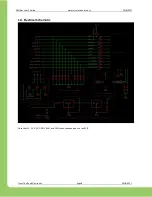
1.2. Pin Descriptions
The CANifier has a multitude of I/O pins. All pins are counted as GPIO (General Purpose Input/Output) except for
power supply pins (5V, GND, 3.3V, VDD).
Pin #
Name
Function
1
SDA
I2C Data pin
2
SCL
I2C Clock pin
3
5V
5V output
4
QUAD A
Quadrature channel A
5
GND
Ground
6
QUAD B
Quadrature channel B
7
INDEX
Quadrature Index
8
LIMF
Limit Switch Forward
9
GND
Ground
10
LIMR
Limit Switch Reverse
11
GND
Ground
12
CS/PWM3
SPI Chip Select / PWM input 3
13
CLK/PWM0
SPI Clock / PWM input 0
14
MOSI/PWM1
SPI Data Out / PWM input 1
15
MISO/PWM2
SPI Data In / PWM input 2
16
5V
5V output
17
5V
5V output
18
3.3V
3.3V output
19
3.3V
3.3V output
20
GND
Ground
21
GND
Ground
CANH
CAN High
CANL
CAN Low
V+
LED Source Voltage (Common anode)
A
LED Channel A (cathode)
B
LED Channel B (cathode)
C
LED Channel C (cathode)
Backside
VDD
Supply Voltage
Backside
GND
Ground


