background image

Disassembly

Removing the LCD Module  2  -  19

2.Disassembly

4.

Remove the screws 

 -


 from the hinge cover and the screws 

 -


 from the hinge (

Figure 14c

).

5.

Remove the LCD module 

 while it is open, still forming a 120 degree angle (

Figure 14d

).

6.

Reverse the process to install a new LCD module.

20

21

22

27

28

d.

c.

28

20

21

22

23

26

27

24

25

28. LCD Module

8  Screws

Figure 14

Top Case Removal 

(cont’d)

c. Remove the screws.
d. Remove the LCD mod-

ule.

Summary of Contents for PA70HS

Page 1: ...PA70HS G PA71HS ...

Page 2: ......

Page 3: ...Preface I Preface Notebook Computer PA70HS G PA71HS Service Manual ...

Page 4: ...hole or in part be reproduced translated transmitted or reduced to any machine readable form without prior consent from the vendor manufacturer or creators of this publica tion except for copies kept by the user for backup purposes Brand and product names mentioned in this publication may or may not be copyrights and or registered trademarks of their respective companies They are mentioned for ide...

Page 5: ...icing and or upgrading components of the PA70HS G PA71HS series notebook PC The following information is included Chapter 1 Introduction provides general information about the location of system elements and their specifications Chapter 2 Disassembly provides step by step instructions for disassembling parts and subsystems and how to upgrade elements of the system Appendix A Part Lists Appendix B ...

Page 6: ...g 3 Do not use the telephone to report a gas leak in the vicinity of the leak 4 Use only the power cord and batteries indicated in this manual Do not dispose of batteries in a fire They may explode Check with local codes for possible special disposal instructions 5 This product is intended to be supplied by a Listed Power Unit as follows AC Input of 100 240V 50 60Hz DC Output of 19 5V 11 8A 230 Wa...

Page 7: ... down properly and don t forget to save your work Remember to periodically save your data as data may be lost if the battery is depleted Do not expose the computer to any shock or vibration Do not place it on an unstable surface Do not place anything heavy on the computer Do not expose it to excessive heat or direct sunlight Do not leave it in a place where foreign matter or mois ture may affect t...

Page 8: ...rpose If you do not have access to a compatible outlet have a qualified electrician install one When you want to unplug the power cord be sure to disconnect it by the plug head not by its wire Make sure the socket and any extension cord s you use can support the total current load of all the connected devices Before cleaning the computer make sure it is disconnected from any external power supplie...

Page 9: ...ur hands or metal objects Battery Guidelines The following can also apply to any backup batteries you may have If you do not use the battery for an extended period then remove the battery from the computer for storage Before removing the battery for storage charge it to 60 70 Check stored batteries at least every 3 months and charge them to 60 70 Battery Disposal The product that you have purchase...

Page 10: ... the DC In jack on the left of the computer then plug the AC power cord into an outlet and connect the AC power cord to the AC DC adapter and leave it there for 6 seconds or longer Remove the adapter cord from the computer s DC In jack and then plug it back in again the battery will now be unlocked 5 Use one hand to raise the lid LCD to a comfortable viewing angle do not exceed 135 degrees use the...

Page 11: ...Preface IX Preface ...

Page 12: ...Preface X Preface ...

Page 13: ...Module 2 11 Removing the Wireless LAN Module 2 14 Wireless LAN Combo Module Cables 2 15 Removing the CCD 2 16 Removing the LCD Module 2 18 Part Lists A 1 Part List Illustration Location A 2 Top A 3 Bottom A 4 Main Board A 5 HDD A 6 LCD A 7 Schematic Diagrams B 1 System Block Diagram B 2 Processor 1 6 B 3 Processor 2 6 B 4 Processor 3 6 B 5 Processor 4 6 B 6 Processor 5 6 B 7 Processor 6 6 B 8 DDR4...

Page 14: ... 53 PEX_VDD B 54 VDD3 VDD5 B 55 DDR 1 2V 0 6VS B 56 Power 1 0V VCCIO B 57 VCC_Core B 58 VCore VCCGT Output B 59 VCCSA B 60 AC_In Charger B 61 NVVDDS B 62 NVVDD 1 B 63 NVVDD 2 B 64 FBVDDQ B 65 LED Board B 66 LID Board B 67 DC Board B 68 Power Board B 69 Click Board B 70 Audio Board B 71 USB Board B 72 USB 3 0 Board B 73 PA7 Card Reader Board 1 4 B 74 PA7 Card Reader Board 2 4 B 75 PA7 Card Reader B...

Page 15: ...l is shipped with the computer Operating systems e g Windows 10 etc have their own manuals as do application softwares e g word processing and database programs If you have questions about those programs you should consult those manuals The PA70HS G PA71HS series notebook is designed to be upgradeable See Disassembly on page 2 1 for a detailed description of the upgrade procedures for each specifi...

Page 16: ...ting frequency depends on the FSB of the processor Memory Expandable from 8GB minimum up to 32GB maximum Compatible with 4GB 8GB or 16GB Modules SO DIMM Memory Types All SO DIMM memory modules installed in the sys tem should be identical the same size and brand in order to prevent unexpected system behavior Do not mix SO DIMM memory module sizes and brands otherwise unexpected system problems may ...

Page 17: ...tel Wireless AC 3168 Wireless LAN 802 11ac Bluetooth Factory Option Qualcomm Atheros Killer Wireless AC 1535 Wireless LAN 802 11ac Bluetooth Factory Option Qualcomm Wireless LAN 802 11ad Bluetooth M 2 Slots Slot WLAN for Combo WLAN and Bluetooth Module Slot SSD1 for SATA or PCIe Gen3 x4 SSD Slot SSD2 for SATA or PCIe Gen3 x2 SSD Intel Optane SSD Module Installation Service personnel please note th...

Page 18: ...nal Locator Top View with LCD Panel Open Figure 1 Top View 1 PC Camera 2 PC Camera LED When the PC camera is in use the LED will be illuminated 3 Built In Array Microphone 4 LCD 5 Speakers 6 Power Button 7 Keyboard 8 Touchpad Buttons 9 Fingerprint Reader Optional 2 1 8 7 6 5 4 5 3 9 3 ...

Page 19: ...Views Figure 2 Front View 1 LED Indicator Figure 3 Right Side View 1 Headphone Out Jack 2 Microphone In Jack 3 Line S PDIF Combo Jack 4 Multi in 1 Card Reader 5 USB 3 0 USB 3 1 Gen 1 Port 6 Powered USB 3 0 USB 3 1 Gen 1 Port 7 RJ 45 LAN Jack 8 Security Lock Slot FRONT VIEW 1 RIGHT SIDE VIEW 1 2 3 7 5 6 4 8 ...

Page 20: ... External Locator Left Side Rear View Figure 4 Left Side View 1 Vent 2 DC In Jack 3 HDMI Out Port 4 Mini Display Port 1 5 Mini Display Port 2 6 USB 3 1 Gen 2 Type C Ports 7 USB 3 0 USB 3 1 Gen 1 Ports LEFT SIDE VIEW 1 2 3 4 5 6 7 Figure 5 Rear View 1 Vent REAR VIEW 1 1 ...

Page 21: ...ottom View 1 7 1 Introduction External Locator Bottom View Figure 6 Bottom View 1 Vent 2 Sub Woofer Overheating To prevent your com puter from overhea ting make sure no thing blocks any vent while the computer is in use 1 2 1 1 1 1 1 ...

Page 22: ...Introduction 1 8 Mainboard Overview Top Key Parts 1 Introduction Mainboard Overview Top Key Parts Figure 7 Mainboard Top Key Parts 2 3 1 ...

Page 23: ...nnector M 2 SSD Module 2 Mini Card Connector M 2 SSD Module 3 KBC ITE IT8587 4 Mini Card Connector WLAN Module 5 PCH 6 GPU GTX1070 7 Memory Slots DDR4 SO DIMM 8 CPU Introduction Mainboard Overview Bottom Key Parts 1 9 1 Introduction Mainboard Overview Bottom Key Parts ...

Page 24: ...rd Overview Top Connectors Figure 9 Mainboard Top Connectors 1 HDMI Port 2 Mini Display Ports 3 USB 3 1 Gen 2 Type C Port 4 Power Connector 5 RGB LED KB Connector 6 RGB LED KB Connector 7 White LED KB Connector 8 Keyboard Cable Connector 9 LID Connector 11 9 7 8 6 5 1 3 4 2 2 ...

Page 25: ...om Connectors 1 Card Reader Board Connector 2 Audio Board Connector 3 Battery Connector 4 VGA Fan Connector 5 HDD Cable Connector 6 FP Cable Connector 7 Click Board Connector 8 USB Board Connector 9 LED Board Connector 10 DC Board Connector 11 CPU Fan Connector 12 LCD Connector 13 CCD Connector 6 8 1 2 4 3 5 11 9 10 1 4 7 10 12 13 ...

Page 26: ...Introduction 1 12 1 Introduction ...

Page 27: ...sassembly process easier each section may have a box in the page margin Information contained under the figure will give a synopsis of the sequence of procedures involved in the disassembly procedure A box with a lists the relevant parts you will have after the disassembly process is complete Note The parts listed will be for the dis assembly procedure listed ONLY and not any previous disassembly ...

Page 28: ...c ing the connection make sure the connector is oriented in the same way The pin1 side is usually not indicated Pressure sockets for multi wire connectors To release this connector type grasp it at its head and gently rock it from side to side as you pull it out Do not pull on the wires themselves When replacing the connection do not try to force it The socket only fits one way Pressure sockets fo...

Page 29: ...the computer When handling a printed circuit board do not use gloves or other materials which allow static electricity buildup We suggest that you use an anti static wrist strap instead 8 Beware of corrosion As you perform your job avoid touching any connector leads Even the cleanest hands produce oils which can attract corrosive elements 9 Keep your work environment clean Tobacco smoke dust or ot...

Page 30: ... battery page 2 6 3 Remove the system memory page 2 10 To remove and install the M 2 SSD 1 Remove the keyboard page 2 5 2 Remove the battery page 2 6 3 Remove the M 2 SSD 1 Intel page 2 11 4 Remove the M 2 SSD 1 page 2 12 5 Remove the M 2 SSD 2 page 2 13 To remove the Wireless LAN Module 1 Remove the keyboard page 2 5 2 Remove the battery page 2 6 3 Remove the WLAN page 2 14 To remove the CCD Modu...

Page 31: ...ing collar socket by using a flat head screwdriver to pry the locking collar pins away from the base Figure 1b 5 Carefully lift the keyboard off the computer Figure 1c 1 2 3 4 5 6 7 7 8 6 a b 1 2 c 6 7 7 8 6 3 4 8 5 8 4 Eject Stick 6 Keyboard 2 Screws Figure 1 Keyboard Removal a Remove the screws from the bottom of the compu ter and then eject the keyboard using a special eject stick to push the k...

Page 32: ...the left thumb to hold down the most prominent area of the back cover and then use the right hand to lift the rear side vent s most prominent area Figure 2c 5 Carefully remove the bottom case up in the direction of the arrow 1 6 2 3 13 14 15 16 17 Figure 2 Battery Removal a Remove the screws b Remove the SD cover and screws c Remove the bottom case a c 2 3 4 5 13 6 15 8 9 11 12 10 b 14 1 7 17 16 2...

Page 33: ...screws Figure 3e 8 Lift the battery off the computer Figure 3f 9 Reverse the process to install a new battery do not forget to replace all the screws and bottom cover 18 19 20 23 24 Figure 3 Battery Removal cont d d Locate the battery e Disconnect the cable and remove the screws f Lift the battery off the computer e f 19 20 22 24 d 18 21 23 24 Battery 4 Screws ...

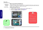
Page 34: ...ocate the HDD b Remove the screws 6 Hard Disk 1 Screw 1 Turn off the computer and remove the keyboard page 2 5 and battery page 2 6 2 The HDD will be visible at point on the mainboard Figure 4a 3 Remove the screw from the HDD assembly Figure 4b 1 2 1 a 2 b HDD System Warning New HDD s are blank Before you begin make sure You have backed up any data you want to keep from your old HDD You have all t...

Page 35: ...gure 5c 6 Remove screws and bracket from the hard disk Figure 5d 7 Reverse the process to install a new hard disk do not forget to replace the screws 3 4 5 6 7 8 c 3 4 d 7 6 5 8 3 HDD Assembly 7 HDD Bracket 8 HDD 2 Screws Figure 5 HDD Assembly Removal cont d c Slide and pull the HDD assembly out of the bay d Remove the screws and bracket from the HDD ...

Page 36: ...the latches to release the second module if necessary 5 Insert a new module holding it at about a 30 angle and fit the connectors firmly into the memory slot 6 The module will only fit one way as defined by its pin alignment Make sure the module is seated as far into the slot as it will go DO NOT FORCE IT it should fit without much pressure 7 Press the module in and down towards the mainboard unti...

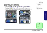
Page 37: ...2 SSD module will be visible at point on the mainboard Figure 7a 3 Remove the screw Figure 7b 4 The M 2 SSD module Figure 7c will pop up and you can remove it from the computer 5 Reverse the process to install a new module do not forget to replace the screws and thermal pad 1 2 3 b c a 2 3 1 3 3 M2 SSD Module 1 Screw Figure 7 M 2 SSD 1 Module Removal a Locate the M 2 SSD b Remove the screw c The M...

Page 38: ...visible at point on the mainboard Figure 7a 3 Remove the screw Figure 7b 4 The M 2 SSD module Figure 7c will pop up and you can remove it from the computer 5 Reverse the process to install a new module do not forget to replace the screws and thermal pad 1 2 3 b c a 2 3 1 3 3 M2 SSD Module 1 Screw Figure 8 M 2 SSD 1 Module Removal a Locate the M 2 SSD b Remove the screw c The M 2 SSD module will po...

Page 39: ...visible at point on the mainboard Figure 7a 3 Remove the screw Figure 7b 4 The M 2 SSD module Figure 7c will pop up and you can remove it from the computer 5 Reverse the process to install a new module do not forget to replace the screws and thermal pad 1 2 3 b c a 2 3 1 3 3 M2 SSD Module 1 Screw Figure 9 M 2 SSD 2 Module Removal a Locate the M 2 SSD b Remove the screw c The M 2 SSD module will po...

Page 40: ...ainboard Figure 10a 3 Carefully disconnect the cables and then remove the screw Figure 10b 4 The Wireless LAN module Figure 10c will pop up and you can remove it from the computer 1 2 3 4 5 b c a 5 1 5 2 3 4 5 Wireless LAN Module 1 Screw Figure 10 Wireless LAN Module Removal a Locate the WLAN b Disconnect the cables and remove the screw c The WLAN module will pop up Note Make sure you reconnect th...

Page 41: ...TE modules are not labelled The cables covers each cable will have either a black or transparent cable cover are color coded for identifi cation as outlined in the table below Cable 1 is usually connected to antenna 1 Main on the module and cable 2 to antenna 2 Aux Module Type Antenna Type Cable Color Cable Cover Type WLAN WLAN Bluetooth Combo WM 1 Black Transparent WM 2 Black White ...

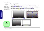
Page 42: ...CD panel to lift it up at points as indicated by the arrows run your fingers again around the inner frame at point to lift from one corner to the other as indicated by the arrows and then lift up the outer frame at point as indicated by the arrows Figure 11e 4 Remove the LCD front cover Figure 11b 1 2 3 4 5 6 7 8 5 b a 9 8 2 1 7 5 6 4 3 9 LCD Front Cover 2 Screws Figure 11 CCD Removal a Remove rub...

Page 43: ...Disassembly 5 Disconnect the cable Figure 12c 6 Remove the CCD module Figure 12d 7 Reverse the process to install a new CCD module 10 11 d c 11 10 11 CCD Module Figure 12 CCD Removal cont d c Disconnect the cable d Remove the CCD mod ule ...

Page 44: ...surface protection pad with the top case open forming a 120 degree angle Carefully disconnect the cables and remove the screws Figure 13a 3 Lift and remove the heatsink from the mainboard Figure 13b 1 4 5 18 19 b a 19 5 2 1 6 7 8 4 3 9 11 12 10 15 13 14 16 17 18 19 Heat sink 14 Screws Figure 13 Top Case Removal a Remove screws and heatsink then carefully release the inner frame of the LCD panel at...

Page 45: ...s from the hinge Figure 14c 5 Remove the LCD module while it is open still forming a 120 degree angle Figure 14d 6 Reverse the process to install a new LCD module 20 21 22 27 28 d c 28 20 21 22 23 26 27 24 25 28 LCD Module 8 Screws Figure 14 Top Case Removal cont d c Remove the screws d Remove the LCD mod ule ...

Page 46: ...und the inner frame at point to lift from one corner to the other as indicated by the arrows and then lift up the outer frame at point as indicated by the arrows Figure 15e 9 Remove the LCD front cover Figure 15f 29 30 31 32 33 34 35 36 37 f e 37 32 30 36 33 35 34 29 31 37 LCD Front Cover 2 Screws Figure 15 LCD Module Removal e Remove rubber and screws and then careful ly release the inner frame o...

Page 47: ...embly 10 Remove the screws Figure 12c 11 Remove the LCD panel Figure 16b 12 Reverse the process to install a new LCD panel 38 41 42 h g 42 38 39 41 40 42 LCD Panel 4 Screws Figure 16 LCD Module Removal cont d g Remove the screws h Remove the LCD panel ...

Page 48: ...Disassembly 2 22 2 Disassembly ...

Page 49: ...bers Your organization may use a different system so be sure to cross check any relevant documentation Note Some assemblies may have parts in common especially screws However the part lists DO NOT indicate the total number of duplicated parts used Note Be sure to check any update notices The parts shown in these illustrations are appropriate for the system at the time of publication Over the produ...

Page 50: ... Illustration Location The following table indicates where to find the appropriate part list illustration Table A 1 Part List Illustration Location Part Top page A 3 Bottom page A 4 Main Board page A 5 HDD page A 6 LCD page A 7 ...

Page 51: ...Top A 3 A Part Lists Top Figure A 1 Top ...

Page 52: ...A 4 Bottom A Part Lists Bottom Figure A 2 Bottom ...

Page 53: ...Main Board A 5 A Part Lists Main Board Figure A 3 Main Board ...

Page 54: ...A 6 HDD A Part Lists HDD Figure A 4 HDD ...

Page 55: ...LCD A 7 A Part Lists LCD Figure A 5 LCD ...

Page 56: ...A 8 A Part Lists ...

Page 57: ...VCCSFR_OC 2 5V Page B 52 USB 3 0 Board Page B 73 Panel Inverter Page B 11 PCH 2 5 Page B 32 1V8_RUN AON NV3V3 Page B 53 PA7 Card Reader Board 1 4 Page B 74 Mini DP Port Back Page B 12 PCH 3 5 Page B 33 PEX_VDD Page B 54 PA7 Card Reader Board 2 4 Page B 75 Mini DP Port Front Page B 13 PCH 4 5 Page B 34 VDD3 VDD5 Page B 55 PA7 Card Reader Board 3 4 Page B 76 HDMI Connector Page B 14 PCH 5 5 Page B 3...

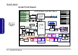
Page 58: ...lia Codec SHEET 55 1 2V VDDQ 0 6VS SHEET 51 SHEET 52 1V8_AON 1V8_RUN NV3V3 AC_IN CHARGER SHEET 60 1 0DX_VCCSTG VCCSFR_OC VPP 2 5V VDD1 0 VCCIO SHEET 56 5V 3 3V 5VS 3VS SHEET 50 SHEET 54 VDD3 VDD5 PEX_VDD SHEET 53 VCC_CORE VCCSA SHEET 57 VCORE OUTPUT STAGE NVVDD SHEET 62 63 NVVDDS SHEET 61 FBVDDQ SHEET 64 INT MIC SHEET 82 37 5x37 5mm 2152 Ball HM175 SHEET 67 LID BOARD K B RGB BACKLIGHT SHEET 36 SHE...

Page 59: ...FWP DP SCHEMATIC1 Title Size Document Number Rev Date Sheet of 6 71 PA700 D02A D02A 02 Processor 1 6 DMI PEG A3 2 77 Wednesday July 05 2017 ᙔ Ϻ ႝ တ DMFWP DP SCHEMATIC1 C739 0 22u_10V_X5R_04 R654 20K_1 _04 C778 0 22u_10V_X5R_04 C774 0 22u_10V_X5R_04 C738 0 22u_10V_X5R_04 C757 0 22u_10V_X5R_04 C756 0 22u_10V_X5R_04 C764 0 22u_10V_X5R_04 C785 0 22u_10V_X5R_04 R533 24 9_1 _04 C736 0 22u_10V_X5R_04 C78...

Page 60: ...1 Title Size Document Number Rev Date Sheet of 6 71 PA700 D02A D02A 03 Processor 2 6 DISPLAY A3 3 77 Wednesday July 05 2017 ᙔ Ϻ ႝ တ DMFWP DP SCHEMATIC1 R477 0_04 R515 24 9_1 _04 R81 1M_04 R99 100K_04 C285 0 1u_10V_X7R_04 C301 0 1u_10V_X7R_04 R98 100K_04 C309 0 1u_10V_X7R_04 C298 0 1u_10V_X7R_04 C336 0 1u_10V_X7R_04 R112 4 7K_04 R79 4 99K_1 _04 R111 4 7K_04 C320 0 1u_10V_X7R_04 C761 0 1u_10V_X7R_04...

Page 61: ...R0_PAR AG3 DDR0_MA 14 DDR0_CAA 9 DDR0_BG 1 AU2 DDR0_MA 15 DDR0_CAA 8 DDR0_ACT AU3 DDR0_MA 13 DDR0_CAB 0 DDR0_MA 13 AE3 DDR0_MA 12 DDR0_CAA 6 DDR0_MA 12 AU4 DDR0_MA 11 DDR0_CAA 7 DDR0_MA 11 AN2 DDR0_MA 8 DDR0_CAA 3 DDR0_MA 8 AN3 DDR0_MA 9 DDR0_CAA 1 DDR0_MA 9 AT4 DDR0_MA 10 DDR0_CAB 7 DDR0_MA 10 AH2 DDR0_MA 6 DDR0_CAA 2 DDR0_MA 6 AP3 DDR0_MA 7 DDR0_CAA 4 DDR0_MA 7 AN1 DDR0_MA 5 DDR0_CAA 0 DDR0_MA 5...

Page 62: ...57 PCH_PECI 31 PCH_CPU_BCLK_R_DN 31 PCH_CPU_BCLK_R_DP 31 PCH_CPU_PCIBCLK_R_DN 31 PCH_CPU_PCIBCLK_R_DP 31 CPU_24MHZ_R_DN 31 CPU_24MHZ_R_DP 31 H_PWRGD 32 PLTRST_CPU_N 31 H_PM_SYNC 31 H_PM_DOWN 31 PCH_THERMTRIP 31 H_SKTOCC_N 32 H_CPU_SVIDCLK 57 H_CPU_SVIDDAT 57 H_CPU_SVIDALRT 57 H_TRST 34 H_PREQ 34 H_PRDY 34 H_PROCHOT_EC 35 H_PECI 35 ALL_SYS_PWRGD 10 34 35 57 DDR_VTT_PG_CTRL 55 1 0DX_VCCSTG 6 51 VDD3...

Page 63: ...L33 RSVD_TP BK24 RSVD_TP BJ24 RSVD BK21 RSVD BJ21 VSS BK18 RSVD_TP BJ34 RSVD_TP BJ33 RSVD G13 RSVD BL31 RSVD F30 RSVD E30 RSVD B30 RSVD C30 RSVD G3 RSVD J3 RSVD BR35 RSVD BR31 RSVD BH30 C452 1u_6 3V_X6S_04 BGA1440 SKYLAKE_HALO U34G SKL_H_CPU VCC P14 VCC V31 VCC V13 VCC V14 VCC U36 VCC U32 VCC U31 VCC U33 VCC U34 VCC U35 VCC T37 VCC T36 VCC U30 VCC U29 VCC T29 VCC T35 VCC T32 VCC R38 VCC R35 VCC R3...

Page 64: ...C9 VSS C8 VSS C5 NCTFVSS C2 NCTFVSS BT36 NCTFVSS BT35 VSS BT32 VSS BT26 VSS BT24 VSS BT21 VSS BT18 VSS BT14 VSS BT12 VSS BT9 VSS BT5 NCTFVSS BT4 NCTFVSS BT3 NCTFVSS BR38 VSS BR36 VSS BR34 VSS BR29 VSS BR26 VSS BR24 VSS BR21 VSS BR18 VSS BR14 VSS BR12 VSS BR7 VSS BP34 VSS BP33 VSS BP29 VSS BP26 VSS BP24 VSS BP21 VSS BP18 VSS BP14 VSS BP12 VSS BP7 VSS BN34 VSS BN31 VSS BN30 VSS BN29 VSS BN24 VSS BN2...

Page 65: ...T0 155 ODT1 161 BG0 115 BG1 113 BA0 150 BA1 145 A0 144 A1 133 A2 132 A3 131 A4 128 A5 126 A6 127 A7 122 A8 125 A9 121 A10_AP 146 A11 120 A12 119 A13 158 A14_WE 151 A15_CAS 156 A16_RAS 152 ACT 114 PARITY 143 ALERT 116 EVENT 134 RESET 108 VREFCA 164 SDA 254 SCL 253 SA2 166 SA1 260 SA0 256 CB0_NC 92 CB1_NC 91 CB2_NC 101 CB3_NC 105 CB4_NC 88 CB5_NC 87 CB6_NC 100 CB7_NC 104 DM0 DBI0 12 DM1 DBI1 33 DM2 ...

Page 66: ...A6 127 A7 122 A8 125 A9 121 A10_AP 146 A11 120 A12 119 A13 158 A14_WE 151 A15_CAS 156 A16_RAS 152 ACT 114 PARITY 143 ALERT 116 EVENT 134 RESET 108 VREFCA 164 SDA 254 SCL 253 SA2 166 SA1 260 SA0 256 CB0_NC 92 CB1_NC 91 CB2_NC 101 CB3_NC 105 CB4_NC 88 CB5_NC 87 CB6_NC 100 CB7_NC 104 DM0 DBI0 12 DM1 DBI1 33 DM2 DBI2 54 DM3 DBI3 75 DM4 DBI4 178 DM5 DBI5 199 DM6 DBI6 220 DM7 DBI7 241 DM8 DBI8 96 S2 C0 ...

Page 67: ...HEMATIC1 Title Size Document Number Rev Date Sheet of 6 71 PA700 D02A D02A 10 PANEL INVERTER A3 10 77 Wednesday July 05 2017 ᙔ Ϻ ႝ တ DMFWP DP SCHEMATIC1 S D G Q4A MTDK3S6R 2 6 1 R76 10K_04 R132 100K_04 C A A D2 BAT54CWH 1 2 3 U5 PI5A3158BZAE P N 6 03 53158 0J1 0B0 2 1B0 11 S0 10 0B1 5 1B1 8 S1 7 VCC 12 A0 1 GND 3 VCC 9 GND 6 A1 4 U23C 74LVC08APW 9 10 8 14 7 R57 4 7K_06 C711 0 1u_10V_X7R_04 C220 0 ...

Page 68: ...7 ᙔ Ϻ ႝ တ DMFWP DP SCHEMATIC1 6 71 PA700 D02A Title Size Document Number Rev Date Sheet of D02A 11 MINI DP PORT BACK _E A3 11 77 Wednesday July 05 2017 ᙔ Ϻ ႝ တ DMFWP DP SCHEMATIC1 6 71 PA700 D02A R683 0_04 C968 0 1u_10V_X7R_04 R627 100K_1 _04 C613 0 01u_50V_X7R_04 C1003 0 1u_10V_X7R_04 U41 uP7549UMA5 20 PCB Footprint M SOT23 5 VOUT 1 VIN 5 GND 2 EN 4 OC 3 R641 0_04 C977 0 1u_10V_X7R_04 C942 10u_6 ...

Page 69: ...U49 PS8330B OUT3N 13 OUT3P 14 DNC 15 OUT2N 16 OUT2P 17 OUT1N 19 OUT1P 20 DNC 21 OUT0P 23 GND 24 V3P3 25 ENABLE ENABLE PD 26 AUX_SNKN 27 AUX_SNKP 28 AUX_SRCN 29 AUX_SRCP 30 GND 31 V3P3 32 SCL_DDC 33 SDA_DDC 34 AUTO EQ RSTN RST 35 V3P3 36 IN2N 45 IN3N 48 EQ DNC CFG1 40 IN1P 41 IN1N 42 IN2P 44 OC_0 DNC NC 46 V3P3 1 HGND 49 DNC VDDD_DREG CEXT 2 OC_1 ADDR_EQ I2C_ADDR 3 OP_0 SCL_CTL SCL_CTL PEQ 4 OP_1 S...

Page 70: ...OCKP 25 HDMI_DATA0N 25 HDMI_DATA0P 25 HDMI_DATA2N 25 HDMI_DATA2P 25 NV3V3 11 12 14 26 46 52 53 61 62 Title Size Document Number Rev Date Sheet of 6 71 PA700 D02A D02A 13 HDMI 2 0 A3 13 77 Wednesday July 05 2017 ᙔ Ϻ ႝ တ DMFWP DP SCHEMATIC1 Title Size Document Number Rev Date Sheet of 6 71 PA700 D02A D02A 13 HDMI 2 0 A3 13 77 Wednesday July 05 2017 ᙔ Ϻ ႝ တ DMFWP DP SCHEMATIC1 Title Size Document Num...

Page 71: ...R_04 C303 0 22u_10V_X5R_04 C133 1u_6 3V_X6S_04 C313 0 22u_10V_X5R_04 C328 0 22u_10V_X5R_04 C155 0 1u_10V_X7R_04 C327 0 22u_10V_X5R_04 R123 10K_04 C165 4 7u_6 3V_X6S_06 1 23 PCI_EXPRESS INS16508609 U22A BK42 PEX_RX15 BL42 PEX_RX15 BG41 PEX_TX15 BH41 PEX_TX15 BM42 PEX_RX14 BM41 PEX_RX14 BG39 PEX_TX14 BF39 PEX_TX14 BL41 PEX_RX13 BK41 PEX_RX13 BE38 PEX_TX13 BF38 PEX_TX13 BK39 PEX_RX12 BL39 PEX_RX12 BH...

Page 72: ... D02A D02A 15 GPU Frame Buffer Partition Custom 15 77 Wednesday July 05 2017 ᙔ Ϻ ႝ တ DMFWP DP SCHEMATIC1 Title Size Document Number Rev Date Sheet of 6 71 PA700 D02A D02A 15 GPU Frame Buffer Partition Custom 15 77 Wednesday July 05 2017 ᙔ Ϻ ႝ တ DMFWP DP SCHEMATIC1 R13 10K_04 R19 60 4_1 _04 R26 10K_04 C107 0 1u_10V_X7R_04 R9 10K_04 R12 10K_04 3 23 FBB INS16511324 U22C Y24 GND Y23 GND Y22 GND Y21 GN...

Page 73: ...Frame Buffer Partition A A3 16 77 Wednesday July 05 2017 ᙔ Ϻ ႝ တ DMFWP DP SCHEMATIC1 Title Size Document Number Rev Date Sheet of 6 71 PA700 D02A D02A 16 Frame Buffer Partition A A3 16 77 Wednesday July 05 2017 ᙔ Ϻ ႝ တ DMFWP DP SCHEMATIC1 R5 40 2_1 _04 INS16516538 M2B K4G80325FB HC25 J10 SEN J13 ZQ J14 VREFC V5 NC_RFU_V5 A5 NC_RFU_A5 J11 CLK J12 CLK J3 CKE J2 RESET J5 RFU_A12 K4 A7_A8 K5 A6_A11 K1...

Page 74: ...2017 ᙔ Ϻ ႝ တ DMFWP DP SCHEMATIC1 Title Size Document Number Rev Date Sheet of 6 71 PA700 D02A D02A 17 Frame Buffer Partition B A3 17 77 Wednesday July 05 2017 ᙔ Ϻ ႝ တ DMFWP DP SCHEMATIC1 Title Size Document Number Rev Date Sheet of 6 71 PA700 D02A D02A 17 Frame Buffer Partition B A3 17 77 Wednesday July 05 2017 ᙔ Ϻ ႝ တ DMFWP DP SCHEMATIC1 NC x16 NORMAL NC NC NC NC NC NC NC x32 NC GND INS16519158 M...

Page 75: ...VSS P10 VSS L5 VSS L10 VSS K14 VSS K1 VSS H14 VSS H1 VSS G5 VSS G10 VSS D10 VSS B5 VSS B10 VSS T3 VDDQ T14 VDDQ T12 VDDQ T1 VDDQ P3 VDDQ P14 VDDQ P12 VDDQ P1 VDDQ N5 VDDQ N10 VDDQ M3 VDDQ M14 VDDQ M12 VDDQ M1 VDDQ L2 VDDQ L13 VDDQ K3 VDDQ K12 VDDQ H3 VDDQ H12 VDDQ G2 VDDQ G13 VDDQ F3 VDDQ F14 VDDQ F12 VDDQ F1 VDDQ E5 VDDQ E10 VDDQ D3 VDDQ D14 VDDQ D12 VDDQ D1 VDDQ B3 VDDQ B14 VDDQ B12 VDDQ B1 VDDQ...

Page 76: ...512 10K_04 GP106 UNUSED GP104 FBD 5 23 FBD INS16530501 U22E Y9 GND Y39 GND Y38 GND Y37 GND Y36 GND Y35 GND Y34 GND Y33 GND M5 FBD_DQS_WP7 U6 FBD_DQS_WP6 H2 FBD_DQS_WP5 E3 FBD_DQS_WP4 AF4 FBD_DQS_WP3 AA9 FBD_DQS_WP2 AG2 FBD_DQS_WP1 AJ3 FBD_DQS_WP0 M9 FBD_DQM7 U5 FBD_DQM6 H3 FBD_DQM5 D3 FBD_DQM4 AD5 FBD_DQM3 AA7 FBD_DQM2 AG1 FBD_DQM1 AJ1 FBD_DQM0 L5 FBD_D63 L4 FBD_D62 L6 FBD_D61 L7 FBD_D60 P5 FBD_D5...

Page 77: ...er Rev Date Sheet of 6 71 PA700 D02A D02A 20 Frame Buffer Partition C A3 20 77 Wednesday July 05 2017 ᙔ Ϻ ႝ တ DMFWP DP SCHEMATIC1 Title Size Document Number Rev Date Sheet of 6 71 PA700 D02A D02A 20 Frame Buffer Partition C A3 20 77 Wednesday July 05 2017 ᙔ Ϻ ႝ တ DMFWP DP SCHEMATIC1 NORMAL x16 NC NC NC NC NC NC NC NC NC NC x32 INS16534713 M6A K4G80325FB HC25 P5 WCK23 P4 WCK23 P2 DBI3 R2 EDC3 M2 DQ...

Page 78: ...r Rev Date Sheet of 6 71 PA700 D02A D02A 21 Frame Buffer Partition D A3 21 77 Wednesday July 05 2017 ᙔ Ϻ ႝ တ DMFWP DP SCHEMATIC1 Title Size Document Number Rev Date Sheet of 6 71 PA700 D02A D02A 21 Frame Buffer Partition D A3 21 77 Wednesday July 05 2017 ᙔ Ϻ ႝ တ DMFWP DP SCHEMATIC1 R160 40 2_1 _04 G2 C801 820p_50V_X7R_04 G2 R151 40 2_1 _04 G2 INS16536547 M7B K4G80325FB HC25 G2 J10 SEN J13 ZQ J14 V...

Page 79: ... C12 VSSQ C11 VSSQ C1 VSSQ A3 VSSQ A14 VSSQ A12 VSSQ A1 VSSQ T5 VSS T10 VSS P10 VSS L5 VSS L10 VSS K14 VSS K1 VSS H14 VSS H1 VSS G5 VSS G10 VSS D10 VSS B5 VSS B10 VSS T3 VDDQ T14 VDDQ T12 VDDQ T1 VDDQ P3 VDDQ P14 VDDQ P12 VDDQ P1 VDDQ N5 VDDQ N10 VDDQ M3 VDDQ M14 VDDQ M12 VDDQ M1 VDDQ L2 VDDQ L13 VDDQ K3 VDDQ K12 VDDQ H3 VDDQ H12 VDDQ G2 VDDQ G13 VDDQ F3 VDDQ F14 VDDQ F12 VDDQ F1 VDDQ E5 VDDQ E10 ...

Page 80: ... C190 1u_6 3V_X6S_04 C215 1u_6 3V_X6S_04 C72 1u_6 3V_X6S_04 C42 10u_4V_X6S_06 C15 10u_4V_X6S_06 C98 10u_4V_X6S_06 C236 1u_6 3V_X6S_04 C259 0 1u_10V_X7R_04 C185 1u_6 3V_X6S_04 C96 1u_6 3V_X6S_04 C154 1u_6 3V_X6S_04 C147 1u_6 3V_X6S_04 C25 22u_6 3V_X6S_08 C46 10u_4V_X6S_06 C158 1u_6 3V_X6S_04 C216 1u_6 3V_X6S_04 C214 1u_6 3V_X6S_04 C238 0 1u_10V_X7R_04 C160 1u_6 3V_X6S_04 C249 1u_6 3V_X6S_04 C169 10...

Page 81: ... DG P 73 recommend Pull down resistor 100k DG P 114 Note PLL power rails trace rounting to GPU BGA ball must be 12 16 mil wide 20mil GPU near GPU under GPU under default Default 1 26 NV CHECK 2016 7 15 Update eDP ID 1 26 NV CHECK GSYNC ID L Strap5 non Gsync L Gsync H aduio playback strapping 嶇P950COST_12 27 GPU_PLLVDD XTALIN XTALOUT XTALOUTBUFF XTALSSIN GND 1V8_AON GND 1V8_AON GND GND GND GND GND ...

Page 82: ... BB15 IFP_IOVDD BB17 IFP_IOVDD BD21 IFPAB_PLLVDD BD23 IFPAB_RSET BK21 IFPB_L0 BL21 IFPB_L0 BM21 IFPB_L1 BM20 IFPB_L1 BL20 IFPB_L2 BK20 IFPB_L2 BK18 IFPB_L3 BL18 IFPB_L3 BH12 IFPB_AUX BG12 IFPB_AUX BG24 IFPA_L0 BF24 IFPA_L0 BE23 IFPA_L1 BF23 IFPA_L1 BH23 IFPA_L2 BG23 IFPA_L2 BG21 IFPA_L3 BF21 IFPA_L3 BG11 IFPA_AUX BH11 IFPA_AUX 11 23 MIOA INS16555158 U22V AM7 MIOA_VREF AM6 MIOACAL_PU_GND AM5 MIOACA...

Page 83: ... 35 60 Title Size Document Number Rev Date Sheet of 6 71 PA700 D02A D02A 26 Misc GPIO_I2C_ROM A3 26 77 Wednesday July 05 2017 ᙔ Ϻ ႝ တ DMFWP DP SCHEMATIC1 Title Size Document Number Rev Date Sheet of 6 71 PA700 D02A D02A 26 Misc GPIO_I2C_ROM A3 26 77 Wednesday July 05 2017 ᙔ Ϻ ႝ တ DMFWP DP SCHEMATIC1 Title Size Document Number Rev Date Sheet of 6 71 PA700 D02A D02A 26 Misc GPIO_I2C_ROM A3 26 77 Wed...

Page 84: ...PA700 D02A D02A 27 NVIDIA POWER SEQUENCE A3 27 77 Wednesday July 05 2017 ᙔ Ϻ ႝ တ DMFWP DP SCHEMATIC1 Title Size Document Number Rev Date Sheet of 6 71 PA700 D02A D02A 27 NVIDIA POWER SEQUENCE A3 27 77 Wednesday July 05 2017 ᙔ Ϻ ႝ တ DMFWP DP SCHEMATIC1 Title Size Document Number Rev Date Sheet of 6 71 PA700 D02A D02A 27 NVIDIA POWER SEQUENCE A3 27 77 Wednesday July 05 2017 ᙔ Ϻ ႝ တ DMFWP DP SCHEMATI...

Page 85: ...DDS_SENSE AP26 VDDS AP25 VDDS AP24 VDDS AP18 VDDS AP17 VDDS AP16 VDDS AP15 VDDS AP14 VDDS AK39 VDDS AK38 VDDS AK37 VDDS AK36 VDDS AK35 VDDS AK29 VDDS AK28 VDDS AK27 VDDS AK26 VDDS AK25 VDDS AK24 VDDS AK18 VDDS AK17 VDDS AK16 VDDS AK15 VDDS AK14 VDDS AG39 VDDS AG38 VDDS AG37 VDDS AG36 VDDS AG35 VDDS AG29 VDDS AG28 VDDS AG27 VDDS AF26 VDDS AF25 VDDS AF24 VDDS AF18 VDDS AF17 VDDS AF16 VDDS AF15 VDDS ...

Page 86: ...AR39 GND AR38 GND AR37 GND AR36 GND AR35 GND AR34 GND AR33 GND AR32 GND AR31 GND AR30 GND AR29 GND AR28 GND AR27 GND AR26 GND AR25 GND AR24 GND AR23 GND AR22 GND AR21 GND AR20 GND B51 GND B5 GND BL34 GND BL31 GND BL28 GND BL25 GND BL22 GND BL2 GND BL19 GND BL16 GND BL13 GND BL10 GND BL1 GND BK1 GND BJ7 GND BJ43 GND BJ42 GND BJ41 GND BJ40 GND BJ39 GND BJ38 GND BJ37 GND BJ36 GND BJ35 GND BJ34 GND BJ...

Page 87: ...FWP DP SCHEMATIC1 Title Size Document Number Rev Date Sheet of 6 71 PA700 D02A D02A 30 PCH 1 5 SPI DMI PCIE USB2 A3 30 77 Wednesday July 05 2017 ᙔ Ϻ ႝ တ DMFWP DP SCHEMATIC1 Title Size Document Number Rev Date Sheet of 6 71 PA700 D02A D02A 30 PCH 1 5 SPI DMI PCIE USB2 A3 30 77 Wednesday July 05 2017 ᙔ Ϻ ႝ တ DMFWP DP SCHEMATIC1 R532 3 3K_1 _04 C833 0 22u_10V_X5R_04 R231 2 2K_04 R559 10K_04 C824 0 22...

Page 88: ...CLK_BIASREF E1 RTCX1 BC9 RTCX2 BD10 GPP_B5 SRCCLKREQ0 BC24 GPP_B6 SRCCLKREQ1 AW24 GPP_B7 SRCCLKREQ2 AT24 GPP_B8 SRCCLKREQ3 BD25 GPP_B9 SRCCLKREQ4 BB24 GPP_B10 SRCCLKREQ5 BE25 GPP_H0 SRCCLKREQ6 AT33 GPP_H1 SRCCLKREQ7 AR31 GPP_H2 SRCCLKREQ8 BD32 GPP_H3 SRCCLKREQ9 BC32 GPP_H4 SRCCLKREQ10 BB31 GPP_H5 SRCCLKREQ11 BC33 GPP_H6 SRCCLKREQ12 BA33 GPP_H7 SRCCLKREQ13 AW33 GPP_H8 SRCCLKREQ14 BB33 GPP_H9 SRCCLK...

Page 89: ...02A 32 PCH 3 5 HDA SMBUS RTC ESP A3 32 77 Wednesday July 05 2017 ᙔ Ϻ ႝ တ DMFWP DP SCHEMATIC1 Title Size Document Number Rev Date Sheet of 6 71 PA700 D02A D02A 32 PCH 3 5 HDA SMBUS RTC ESP A3 32 77 Wednesday July 05 2017 ᙔ Ϻ ႝ တ DMFWP DP SCHEMATIC1 R519 10K_04 R570 0_04 R523 1K_04 R489 51_04 R561 10K_04 R498 51_04 R565 1K_04 R197 1K_04 R553 10K_04 JOPEN1 OPEN_10mil 1MM 1 2 R518 22_04 R589 1K_04 R57...

Page 90: ...PRIM_1P0 AJ20 VCCPRIM_1P0 AC23 VCCPRIM_1P0 AC26 VCCPRIM_1P0 AC28 VCCPRIM_1P0 AE23 VCCPRIM_1P0 AE26 VCCPRIM_1P0 Y23 VCCPRIM_1P0 Y25 DCPRTC BA26 VCCCLK1 N17 C384 1u_6 3V_X5R_04 C795 0 1u_10V_X7R_04 C415 0 1u_10V_X7R_04 C422 0 1u_10V_X7R_04 C424 1u_6 3V_X5R_04 L4 HCB1608KF 121T30 SPT H_PCH U30I HM175 VSS AE29 VSS AE4 VSS AE42 VSS AF18 VSS AF20 VSS AF21 VSS AF23 VSS AF25 VSS AF26 VSS AF28 VSS AF29 VSS...

Page 91: ... 34 PCH 5 5 UART I2C GPIO A3 34 77 Wednesday July 05 2017 ᙔ Ϻ ႝ တ DMFWP DP SCHEMATIC1 Title Size Document Number Rev Date Sheet of 6 71 PA700 D02A D02A 34 PCH 5 5 UART I2C GPIO A3 34 77 Wednesday July 05 2017 ᙔ Ϻ ႝ တ DMFWP DP SCHEMATIC1 C428 0 1u_10V_X7R_04 R491 0_04 R584 10K_04 SPT H_PCH U30K HM175 GPP_B22 GSPI1_MOSI AT29 GPP_B21 GSPI1_MISO AR29 GPP_B20 GSPI1_CLK AV29 GPP_B19 GSPI1_CS BC27 GPP_B1...

Page 92: ... 2017 ᙔ Ϻ ႝ တ DMFWP DP SCHEMATIC1 R712 47_04 Q46 BTN3904 M SOT23 CBE B E C C1056 0 1u_10V_X7R_04 R661 100K_04 D42 BAV99 RECTIFIER A C AC R636 10K_04 Q45 2SK3018S3 G D S C920 1u_6 3V_X5R_04 R626 20K_1 _04 J_KB1 85208 24051 PA50 24 23 22 14 12 11 21 8 20 19 6 5 18 4 17 10 9 7 3 2 1 16 15 13 R644 0_04 R711 47_04 C914 0 1u_10V_X7R_04 R648 10K_04 C955 10u_6 3V_X5R_06 C975 0 1u_10V_X7R_04 J_KB2 85208 24...

Page 93: ...VGA_THERM 26 35 44 SMD_VGA_THERM 26 35 44 KBLED_DET 32 KBLIGHT_ADJ 35 BOTZONE_DET 34 Title Size Document Number Rev Date Sheet of 6 71 PA700 D02A D02A 36 RGB AND WHITE KB LED 36 77 Wednesday July 05 2017 ᙔ Ϻ ႝ တ DMFWP DP SCHEMATIC1 A3 Title Size Document Number Rev Date Sheet of 6 71 PA700 D02A D02A 36 RGB AND WHITE KB LED 36 77 Wednesday July 05 2017 ᙔ Ϻ ႝ တ DMFWP DP SCHEMATIC1 A3 Title Size Docu...

Page 94: ...Sheet of 6 71 PA700 D02A D02A 37 M 2 PCIE4X SSD_1 2X SSD_2 A3 37 77 Wednesday July 05 2017 ᙔ Ϻ ႝ တ DMFWP DP SCHEMATIC1 C873 0 1u_10V_X7R_04 C918 0 1u_10V_X7R_04 C1028 0 1u_10V_X7R_04 R809 0_04 C1012 0 1u_10V_X7R_04 R804 1K_04 M KEY J_SSD1 NFSM0 S6701 TP64 PCB Footprint NXSM0 S67XX XX40 SUSCLK 32Khz O 68 CLKREQ IO 52 GND11 71 REFCLKP 55 REFCLKN 53 PEWake IO 54 PEDET NC PCIe GND SATA 69 GND10 57 DAS...

Page 95: ...GR8 10K_04 3G GC14 47u_6 3V_X5R_08 GL2 WCM2012F2S SHORT 1 4 2 3 R795 0_04 GQ1 2SK3018S3 3G G D S R214 0_04 GC13 0 1u_10V_X7R_04 3G GQ2A MTS3572G6 3G S2 4 D2 3 G2 5 C836 0 1u_10V_X7R_04 C818 0 1u_10V_X7R_04 GL3 WCM2012F2S SHORT 1 4 2 3 R796 0_04 GR7 0_04 3G GC6 0 1u_10V_X7R_04 3G C848 22u_6 3V_X5R_08 GR3 330K_04 3G GL1 WCM2012F2S SHORT 1 4 2 3 GR5 10_06 3G C814 0 1u_10V_X7R_04 R211 10K_04 R797 0_04...

Page 96: ...ATA 47 MIC_CLK 47 SPDIFO 48 HEADPHONE R 48 HEADPHONE L 48 SMB_CLK 32 47 55 SMB_DATA 32 47 55 HP_JSGND 48 Title Size Document Number Rev Date Sheet of 6 71 PA700 D02A D02A 39 audio 892 A3 39 77 Wednesday July 05 2017 Title Size Document Number Rev Date Sheet of 6 71 PA700 D02A D02A 39 audio 892 A3 39 77 Wednesday July 05 2017 Title Size Document Number Rev Date Sheet of 6 71 PA700 D02A D02A 39 audi...

Page 97: ...14 0 1u_10V_X7R_04 Function SJ_SUBWOOF1 88266 02001 2 1 SC5 1000p_50V_X7R_04 Function SC9 0 1u_10V_X7R_04 Function SC18 10u_6 3V_X5R_06 Function SD1 FMS3004 AS H Function A C SR30 100K_04 Function SC12 0 1u_10V_X7R_04 Function SC27 0 1u_10V_X7R_04 Function SR33 4 32K_1 _04 Function SR35 10K_04 Function SC19 10u_6 3V_X5R_06 Function SC30 0 1u_10V_X5R_04 Function SR38 10K_04 Function SR22 18K_1 _06 ...

Page 98: ...5 2017 Title Size Document Number Rev Date Sheet of 6 71 PA700 D02A D02A 41 audio 892 PORT1 A3 41 77 Wednesday July 05 2017 Title Size Document Number Rev Date Sheet of 6 71 PA700 D02A D02A 41 audio 892 PORT1 A3 41 77 Wednesday July 05 2017 C951 22u_6 3V_X5R_08 R266 100K_04 R267 0_04 C945 0 1u_10V_X7R_04 R304 120K_04 C581 220p_50V_NPO_04 J_SPK1 88266 04001 PCB Footprint 88266 04_L 1 2 3 4 C565 100...

Page 99: ...2 35 38 48 Title Size Document Number Rev Date Sheet of 6 71 PA700 D02A D02A 42 AR_TBT A3 42 77 Wednesday July 05 2017 Title Size Document Number Rev Date Sheet of 6 71 PA700 D02A D02A 42 AR_TBT A3 42 77 Wednesday July 05 2017 Title Size Document Number Rev Date Sheet of 6 71 PA700 D02A D02A 42 AR_TBT A3 42 77 Wednesday July 05 2017 R311 2 2K_1 _04 C585 0 1u_6 3V_X5R_02 R332 100_04 C614 0 22u_10V_...

Page 100: ...5 VSS_ANA J19 VSS_ANA J20 VSS_ANA L5 VSS_ANA J18 VSS_ANA J22 VSS_ANA J23 VSS_ANA K1 VSS_ANA K2 VSS_ANA L20 VSS_ANA L22 VSS_ANA L23 VSS_ANA M1 VSS_ANA M2 VSS_ANA M5 VSS_ANA M19 VSS_ANA M20 VSS_ANA N5 VSS_ANA N20 VSS_ANA N22 VSS_ANA N23 VSS_ANA AA22 VSS_ANA AA23 VSS_ANA AB6 VSS_ANA AB8 VSS_ANA AB10 VSS_ANA AB12 VSS_ANA AB14 VSS_ANA AB16 VSS_ANA AB18 VSS_ANA AB20 VSS_ANA AB22 VSS_ANA AC6 VSS_ANA AC8 ...

Page 101: ...4 TBT R769 1M_04 TBT R819 0_04 FUNCTION R780 100K_04 TBT R782 0_04 FUNCTION C658 1u_25V_X5R_06 TBT L13 HCB2012KF 800T80 TBT FUNCTION R767 100K_04 TBT R385 100K_04 TBT C649 2 2u_6 3V_X5R_04 TBT R783 10K_04 TBT EMR2 0_04 R820 0_04 FUNCTION FUNCTION C1134 10u_6 3V_X5R_04 TBT C644 1u_6 3V_X5R_04 TBT R401 10K_04 TBT R376 100K_04 TBT R766 100K_04 TBT R816 0_04 TBT C1138 22u_6 3V_X5R_08 R790 0_04 FUNCTIO...

Page 102: ..._R 44 TBTA_HD2CA_1_N_R 44 TBTA_HD2CA_1_P_R 44 TBTA_SBU2_J 44 TBTA_SBU1_J 44 TBTA_CC2_J 44 TBTA_CC1_J 44 TBTA_USB2_BP_J 44 TBTA_USB2_BN_J 44 TBTA_USB2_TN_J 44 TBTA_USB2_TP_J 44 3 3V 2 10 27 38 43 48 50 51 52 55 56 5V 39 44 48 49 50 51 52 53 54 55 56 57 58 59 63 TBTA_VBUS 44 Title Size Document Number Rev Date Sheet of 6 71 PA700 D02A D02A 45 USB3 0 co lay TYPE C A3 45 77 Wednesday July 05 2017 ᙔ Ϻ ...

Page 103: ...N_D0p IN_D0n IN_D1n MDP_E 3 MDP_E3 MDP_E 2 MDP_E2 MDP_E 1 MDP_E1 MDP_E 0 MDP_E0 IN_AUXn GND IN_CA_DET IN_AUXp MUX_AUXN MUX_AUXP 3 3VS 3 3VS 3 3VS 3 3VS 3 3VS 3 3VS 3 3VS 3 3VS 3 3VS 3 3VS 3 3VS NV3V3 NV3V3 NV3V3 3 3VS 3 8 9 10 11 12 13 26 30 31 32 33 34 35 36 37 38 39 41 43 47 48 49 50 57 64 NV3V3 11 12 13 14 26 52 53 61 62 OUT1_AUXp_SCL 11 OUT1_AUXn_SDA 11 OUT1_D0p 11 OUT1_D0n 11 OUT1_D1p 11 OUT1...

Page 104: ... A3 47 77 Wednesday July 05 2017 ᙔ Ϻ ႝ တ DMFWP DP SCHEMATIC1 H30 H6_0D2_8 R710 0_04 H15 H9_5D6_0 C677 47p_50V_NPO_04 H20 H8_0D3_7 H6 H6_3D4_4 H18 H9_5D6_0 C1139 47p_50V_NPO_04 C1114 0 1u_10V_X7R_04 R221 100K_04 W O TPM H11 H9_5D6_0 H12 H8_0D2_8 R708 10K_04 C663 1u_6 3V_X5R_04 H33 H8_0D2_8 R758 0_04 S D G Q27B MTDK3S6R 5 3 4 C1140 47p_50V_NPO_04 H29 C111D111N M13 M MARK R352 2 2K_04 H23 H8_0D2_8 H3...

Page 105: ...35 37 38 42 47 DD_ON 50 55 LAN_WAKEUP 30 32 35 38 42 HEADPHONE L 39 HP_JSGND 39 SIDE_R 39 SIDE_L 39 JD_SENSEA 39 JD_SENSEB 39 MIC1_R_M 39 MIC1_L_M 39 USB_PN6 30 USB_PP6 30 USB_PN4 30 USB_PP4 30 DD_ON 35 45 50 54 USB_PP1 30 USB_PN1 30 USB3_RXP1 32 USB3_RXN1 32 USB3_TXN1 32 USB3_TXP1 32 USB_PN5 30 USB_PP5 30 USB3_RXN5 32 USB3_RXP5 32 UIM_RST 38 UIM_PWR 38 UIM_DATA 38 UIM_CLK 38 SIM_DET 38 SPDIFO 39 ...

Page 106: ...cument Number Rev Date Sheet of 6 71 PA700 D02A D02A 49 FAN LID SATA HDD A3 49 77 Wednesday July 05 2017 ᙔ Ϻ ႝ တ DMFWP DP SCHEMATIC1 Title Size Document Number Rev Date Sheet of 6 71 PA700 D02A D02A 49 FAN LID SATA HDD A3 49 77 Wednesday July 05 2017 ᙔ Ϻ ႝ တ DMFWP DP SCHEMATIC1 C750 1u_6 3V_X5R_04 C931 0 1u_10V_X7R_04 C952 1u_6 3V_X5R_04 Q50 2SK3018S3 G D S C745 4 7u_6 3V_X5R_06 J1 OPEN 3mm 1 2 C7...

Page 107: ...0 77 Wednesday July 05 2017 ᙔ Ϻ ႝ တ DMFWP DP SCHEMATIC1 R800 10K_04 S D G Q54B MTDK3S6R 5 3 4 PR337 100K_04 PR358 10K_04 C701 0 1u_50V_Y5V_06 R22 10K_04 PC215 0 1u_10V_X7R_04 PJ37 1mm 1 2 S D G Q54A MTDK3S6R 2 6 1 PR352 100K_04 C450 1u_6 3V_X5R_04 C470 0 1u_10V_X7R_04 G5016 U12 CT2 10 OUT2 8 EN2 5 VBIAS 4 IN2 6 GND 11 EN1 3 CT1 12 OUT1 13 IN1 1 IN1 2 OUT1 14 IN2 7 OUT2 9 GND 15 C89 0 01u_50V_X7R_0...

Page 108: ...y July 05 2017 ᙔ Ϻ ႝ တ DMFWP DP SCHEMATIC1 Title Size Document Number Rev Date Sheet of 6 71 PA700 D02A D02A 51 1 0DX_VCCSTG VCCSFR_OC 2 5 A3 51 77 Wednesday July 05 2017 ᙔ Ϻ ႝ တ DMFWP DP SCHEMATIC1 Title Size Document Number Rev Date Sheet of 6 71 PA700 D02A D02A 51 1 0DX_VCCSTG VCCSFR_OC 2 5 A3 51 77 Wednesday July 05 2017 ᙔ Ϻ ႝ တ DMFWP DP SCHEMATIC1 PC181 10u_6 3V_X5R_06 PC180 0 1u_10V_X7R_04 P...

Page 109: ...tle Size Document Number Rev Date Sheet of 6 71 PA700 D02A D02A 52 1V8_RUN 1V8_AON NV3V3 A3 52 77 Wednesday July 05 2017 ᙔ Ϻ ႝ တ DMFWP DP SCHEMATIC1 C779 100p_50V_NPO_04 R481 0_04 PC169 1u_6 3V_X5R_04 PR277 10K_1 _04 D23 RB0540S2 A C C771 10u_6 3V_X5R_06 PR284 10K_1 _04 PR281 0_04 R125 10_06 PC172 0 22u_10V_X5R_04 PR276 10_06 S D G Q13A MTDK3S6R 2 6 1 C331 10u_6 3V_X5R_06 C781 1u_6 3V_X5R_04 PC171...

Page 110: ...7 PS2_FBVDDQ_FB 64 I2CC_SCL 26 53 VIN 10 35 39 50 54 55 56 57 58 59 60 VDD3 5 26 30 31 32 33 34 35 37 38 48 49 50 51 52 54 56 59 60 PEX_VDD 14 25 NV3V3 11 12 13 14 26 46 52 61 62 5V 39 44 45 48 49 50 51 52 54 55 56 57 58 59 63 1V8_RUN 14 15 23 24 28 52 3 3V 2 10 27 38 43 45 48 50 51 52 55 56 PWR_SRC_NV_FB 61 62 64 PWR_SRC_NV 62 63 1V8_AON 3 23 24 26 27 28 31 52 61 62 64 I2CC_SCL 26 53 PWR_SRC_NVS_...

Page 111: ...mm 1 2 PC225 1000p_50V_X7R_04 PC192 220u_6 3V_6 3 4 4 PR339 0_04 R606 5 1_06 PQ35 MDU1516 ULTRASO 8 G D S PR356 0_04 PR338 0_04 PC222 0 1u_10V_X7R_04 PQ33 QM3006M3 4 5 2 5 5 3 1 5 PC207 0 1u_50V_Y5V_06 PR343 0_04 PR355 13 7K_1 _04 PC211 1u_10V_X7R_06 PR362 100K_04 PC213 0 1u_10V_X7R_04 PR351 19 1K_1 _06 PC221 1u_10V_Y5V_06 PC223 100p_50V_NPO_04 PC216 1000p_50V_X7R_04 PR349 60 4K_1 _04 PQ40 2SK3018...

Page 112: ...00K_04 PR146 0_04 PL20 BCIHP0730 1R0M PCB Footprint BCIHP0735A 1 2 PR370 47K_04 PJ49 8mm 1 2 PR147 10K_04 PQ50 2SK3018S3 G D S Q24 2SK3018S3 G D S PR379 15mil_short PR402 0_04 PC242 330uF_2V_5 5 4 2 PJ51 CV 40mil 1 2 R723 0_04 PQ46 MDU1516 ULTRASO 8 G D S PR364 100K_04 R719 0_04 C981 0 22u_10V_X5R_04 C1048 1u_6 3V_X5R_04 R666 10K_04 PC267 0 1u_50V_Y5V_06 R675 0_04 PR391 0_04 PD24 RB0540S2 A C PQ52...

Page 113: ... July 05 2017 ᙔ Ϻ ႝ တ DMFWP DP SCHEMATIC1 C803 0 1u_10V_X7R_04 PC191 15p_50V_NPO_04 PC201 0 01u_16V_X7R_04 PJ38 CV 40mil 1 2 R568 5 1_06 PJ12 1mm 1 2 PQ32 QM3004M3 4 5 2 5 5 3 1 5 C868 0 01u_16V_X7R_04 PJ14 3mm 1 2 PR307 6 19K_1 _04 PJ42 CV 40mil 1 2 PJ40 6mm 1 2 PR316 820K_1 _06 C375 0 1u_10V_X7R_04 R149 100_04 G5016 U9 CT2 10 OUT2 8 EN2 5 VBIAS 4 IN2 6 GND 11 EN1 3 CT1 12 OUT1 13 IN1 1 IN1 2 OUT...

Page 114: ...PR103 0_04 PR106 10_04 PC68 1000p_50V_X7R_04 PR322 806_1 _04 PC73 1000p_50V_X7R_04 PR318 1K_1 _04 PR118 100_04 PR109 1_04 PR320 5 9K_1 _04 PR124 680_1 _04 GND 57 PU4 RT3606BEGQW ISEN3N 3 PS4 43 VCLK 23 IMONA 19 VSEN 10 ISEN2N 7 ISEN3P 2 ISEN1N 4 NC 40 SET2 13 COMPA 31 FBA 32 RGNDA 29 SETA2 16 VSENA 30 OFSA PSYS 26 IBIAS 28 ISENA1P 35 SET1 12 PGOOD 47 SETA1 15 PWMA1 42 EN 24 ISEN2P 6 ALERT 21 ISEN1...

Page 115: ...P PC212 1u_16V_X7R_06 PC189 2200p_50V_X7R_04 PC220 4 7u_25V_X7R_08 PR89 374_1 _04 PC230 4 7u_25V_X7R_08 PR383 20mil_04 PR350 20mil_04 PC210 0 1u_25V_X7R_06 PQ42 SM7320ESQG 1 2 8 3 4 9 5 6 7 PL13 CMME063T R15MS0R907 1 2 PR384 2 2_1 _06 INS16653671 PQ30 CSD87350Q5D 1 D1 2 3 G1 4 S1 5G2 6 D2 7 8 9 S2 PR90 20mil_04 PC226 4 7u_25V_X7R_08 PC217 1u_25V_X7R_06 PC243 390uF_2 5V_10m_6 3 6 PR336 1_1 _06 PC22...

Page 116: ...17 ᙔ Ϻ ႝ တ DMFWP DP SCHEMATIC1 Title Size Document Number Rev Date Sheet of 6 71 PA700 D02A D02A 59 VCCSA Power A3 59 77 Wednesday July 05 2017 ᙔ Ϻ ႝ တ DMFWP DP SCHEMATIC1 PC56 0 01u_16V_X7R_04 PJ29 8mm 1 2 PR83 100_04 PC54 0 1u_10V_X7R_04 PR86 100_04 PC163 330uF_2V_5 5 4 2 PJ9 1mm 1 2 PR77 820K_1 _06 PR74 0_06 PC55 0 1u_50V_Y5V_06 PQ26 QM3006M3 4 5 2 5 5 3 1 5 PU3 G5602R41U VOUT 1 EN_PSV 15 TON 1...

Page 117: ...0SRUYR ACN 1 ACP 2 CMSRC 3 ACDRV 4 ACOK 5 ACDET 6 IADP 7 IDCHG 8 PMON 9 PROCHOT 10 SDA 11 SCL 12 CMPIN 13 CMPOUT 14 BATPRES 15 TB_STAT 16 BATSRC 17 BATDRV 18 SRN 19 SRP 20 ILIM 21 GND_1 22 LODRV 23 REGN 24 BTST 25 HIDRV 26 PHASE 27 VCC 28 GND_2 29 PC287 1000p_50V_X7R_04 PR381 10_1 _06 PR145 10K_04 PC253 1u_25V_X5R_06 PC293 2 2u_25V_X5R_08 PRS4 0 01_1 _32 PC280 1u_25V_X5R_06 J_DC_JACK1 50299 00801 ...

Page 118: ... 1500p_50V_04 PR46 0_04 PD13 CSOD140SH G2 A C PC50 4700p_50V_X7R_04 PC45 1u_6 3V_X5R_04 PR261 0_04 PR260 0_04 PR68 45 3K_1 _04 PC39 4 7u_25V_X7R_08 G2 PC134 330uF_2V_5 5 4 2 PR250 100K_04 G2 PD1 CSOD140SH A C PR65 0_04 PC140 330uF_2V_5 5 4 2 PR264 309_1 _04 PR263 16 5K_1 _04 PL8 CMME063T R24MS1R197 1 2 PQ2 QM3006M3 4 5 2 5 5 3 1 5 PC145 2200p_50V_X7R_04 G2 PC142 4 7u_25V_X7R_08 G2 PR255 62K_1 _04 ...

Page 119: ... 1 2 PR15 20K_1 _04 PC26 1u_25V_X7R_06 PR191 100K_1 _04 PR17 499_1 _04 PR187 0_04 PR194 10K_04 PR189 499_1 _04 PR174 0_04 PC98 1u_25V_X7R_06 PR195 2_1 _04 PR178 4 32K_1 _04 PR171 0_04 PR173 15K_1 _04 PR11 309_1 _04 PC112 0 1u_25V_X7R_06 PR21 15K_1 _04 PR181 1K_04 PC4 0 01u_50V_X7R_04 PC116 0 1u_25V_X7R_06 PC21 25TQC15MYFB PRS1 RL1632T4F B R005 FNH 1 2 3 4 PR190 10K_04 PR10 51K_1 _04 PR202 10K_04 P...

Page 120: ...5R_08 PU6 UP1909PDN8 G2 BST 2 PWM 3 EN 7 VCC 6 DRVH 1 SW 8 PGND 4 DRVL 5 GND 9 PC14 4 7u_25V_X7R_08 INS16668508 PQ16 CSD87350Q5D 1 D1 2 3 G1 4 S1 5G2 6 D2 7 8 9 S2 PR156 0_04 C37 22u_6 3V_X5R_08 PR160 15_1 _06 C693 22u_6 3V_X5R_08 PR165 2_1 _04 PR166 0_04 PC294 1000p_50V_X7R_04 PC27 220u_2V_SMD V C23 22u_6 3V_X5R_08 PC133 330uF_2V_5 5 4 2 PC113 2200p_50V_X7R_04 PC15 4 7u_25V_X7R_08 PR163 15_1 _06 ...

Page 121: ...PR219 75K_1 _04 PC121 0 1u_10V_X7R_04 PC104 4 7u_25V_X7R_08 PR206 2 2_04 PR7 78 7K_1 _04 PR227 1K_04 PR207 0_04 PC94 0 1u_10V_X7R_04 PR239 100_04 PR214 0_04 PR232 0_04 PR241 10K_04 PR229 0_04 PR235 4 99K_1 _04 PC1 0 01u_50V_X7R_04 PC106 0 1u_50V_Y5V_06 PR192 5 1_06 PR240 0_04 PR218 0_04 PR221 100K_04 PQ15 SM7320ESQG 1 2 8 3 4 9 5 6 7 PQ20 SM7320ESQG 1 2 8 3 4 9 5 6 7 PR230 0_04 PR9 15_1 _06 PC82 1...

Page 122: ...OARD_M A3 65 77 Wednesday July 05 2017 ᙔ Ϻ ႝ တ DMFWP DP SCHEMATIC1 Title Size Document Number Rev Date Sheet of 6 71 PA704 D02A D02A 65 PA7 LED BOARD_M A3 65 77 Wednesday July 05 2017 ᙔ Ϻ ႝ တ DMFWP DP SCHEMATIC1 Title Size Document Number Rev Date Sheet of 6 71 PA704 D02A D02A 65 PA7 LED BOARD_M A3 65 77 Wednesday July 05 2017 ᙔ Ϻ ႝ တ DMFWP DP SCHEMATIC1 MR5 220_04 MR4 680_04 5MR1 0_04 MR2 680_04 ...

Page 123: ... Wednesday July 05 2017 ᙔ Ϻ ႝ တ DMFWP DP Title Size Document Number Rev Date Sheet of 6 71 PA706 D02A D02A 66 LID BOARD_V A3 66 77 Wednesday July 05 2017 ᙔ Ϻ ႝ တ DMFWP DP 3VR1 0_04 6VR1 0_04 VH3 H4_0D2_2 VR1 100K_04 4VR1 0_04 VD1 V15AVLC0402 1 2 VJ_LID1 FPC1004 4AW S PCB Footprint FP226H 004XXXM_R 1 2 3 4 NC1 NC2 2VR1 0_04 VU1 AH9249NTR G1 VCC 1 OUT 2 GND 3 1VR1 0_04 VC1 100p_50V_NPO_04 5VR1 0_04 ...

Page 124: ...Number Rev Date Sheet of 6 71 PA70C D02A D02A 67 DC BOARD_D A3 67 77 Wednesday July 05 2017 ᙔ Ϻ ႝ တ DMFWP DP SCHEMATIC1 Title Size Document Number Rev Date Sheet of 6 71 PA70C D02A D02A 67 DC BOARD_D A3 67 77 Wednesday July 05 2017 ᙔ Ϻ ႝ တ DMFWP DP SCHEMATIC1 6DR1 0_04 DH2 H7_0D2_3 DJ_DC_JACK2 207B07BHB0A PCB Footprint 2DC G213 B48 1 2 GND1 GND2 GND4 GND3 5DR1 0_04 3DR1 0_04 2DR1 0_04 DJ_DC_JACK1 ...

Page 125: ... တ DMFWP DP SCHEMATIC1 Title Size Document Number Rev Date Sheet of 6 71 PA70S D02A D02A 68 POWER BOARD_B A3 68 77 Wednesday July 05 2017 ᙔ Ϻ ႝ တ DMFWP DP SCHEMATIC1 Title Size Document Number Rev Date Sheet of 6 71 PA70S D02A D02A 68 POWER BOARD_B A3 68 77 Wednesday July 05 2017 ᙔ Ϻ ႝ တ DMFWP DP SCHEMATIC1 BH4 H4_0D2_2 BJ_BTN1 FPC1004 4AW S fp226h 004xxxm_l 1 2 3 4 NC1 NC2 BH1 H4_0D2_2 3BR1 0_04 ...

Page 126: ...itle Size Document Number Rev Date Sheet of 6 71 PA702 D02A D02A 69 PA7 CLICK BOARD_T A3 69 77 Wednesday July 05 2017 ᙔ Ϻ ႝ တ DMFWP DP SCHEMATIC1 Title Size Document Number Rev Date Sheet of 6 71 PA702 D02A D02A 69 PA7 CLICK BOARD_T A3 69 77 Wednesday July 05 2017 ᙔ Ϻ ႝ တ DMFWP DP SCHEMATIC1 Title Size Document Number Rev Date Sheet of 6 71 PA702 D02A D02A 69 PA7 CLICK BOARD_T A3 69 77 Wednesday J...

Page 127: ...July 05 2017 ᙔ Ϻ ႝ တ DMFWP DP SCHEMATIC1 Title Size Document Number Rev Date Sheet of 6 71 PA708 D02A D02A 70 AUDIO BOARD_E A3 70 77 Wednesday July 05 2017 ᙔ Ϻ ႝ တ DMFWP DP SCHEMATIC1 EH3 H4_2D2_2 EC8 100p_50V_NPO_04 ER12 39 2K_1 _04 5ER1 0_04 EJ_MIC1 2SJ3006 008311F 4 3 2 5 1 ER5 22K_04 6ER1 0_04 EH2 H4_2D2_2 ER13 5 1K_1 _04 EJ_HP1 2SJ3006 008311F 4 3 2 5 1 ER6 22K_04 EL4 FCM1005KF 121T03 EL2 FCM...

Page 128: ..._W A3 71 77 Wednesday July 05 2017 ᙔ Ϻ ႝ တ DMFWP DP Title Size Document Number Rev Date Sheet of 6 71 PA703 D12A D02A 71 USB3 0 BOARD_W A3 71 77 Wednesday July 05 2017 ᙔ Ϻ ႝ တ DMFWP DP WC7 22u_6 3V_X5R_08 WC10 0 1u_10V_X7R_04 3WR1 0_04 WD2 TVUDF1004AD0 5 1 2 3 4 10 9 8 7 6 WC6 22u_6 3V_X5R_08 WC5 22u_6 3V_X5R_08 WU1 uP7549UMA5 20 PCB Footprint M SOT23 5 VOUT 1 VIN 5 GND 2 EN 4 OC 3 WH1 H8_0D2_8 2W...

Page 129: ...1 VIN 5 GND 2 EN 4 OC 3 ZC7 0 1u_10V_X7R_04 ZR10 4 7K_04 1ZR1 0_04 ZR5 0_04 ZC41 4 7K_04 ZC25 0 1u_10V_X7R_04 ZC4 22u_6 3V_X5R_08 ZH3 H5_0D2_2 ZH1 H8_0D2_8 ZR2 4 7K_04 ZH2 H5_0D2_2 ZC28 4 7K_04 ZC21 0 1u_10V_X7R_04 ZD1 TVUDF1004AD0 5 1 2 3 4 10 9 8 7 6 ZC1 10u_6 3V_X5R_06 ZR3 4 7K_04 ZC29 0_04 ZR9 4 7K_04 ZC15 0 1u_10V_X7R_04 ZJ_USB1 FP225H 030S10M PCB Footprint FP225H 030GXXM 1 1 2 2 3 3 4 4 5 5 ...

Page 130: ...PA70Z D02A D02A 73 PA7 LAN BOARD_N 1 4 A3 73 77 Wednesday July 05 2017 ᙔ Ϻ ႝ တ DMFWP DP SCHEMATIC1 Title Size Document Number Rev Date Sheet of 6 71 PA70Z D02A D02A 73 PA7 LAN BOARD_N 1 4 A3 73 77 Wednesday July 05 2017 ᙔ Ϻ ႝ တ DMFWP DP SCHEMATIC1 Title Size Document Number Rev Date Sheet of 6 71 PA70Z D02A D02A 73 PA7 LAN BOARD_N 1 4 A3 73 77 Wednesday July 05 2017 ᙔ Ϻ ႝ တ DMFWP DP SCHEMATIC1 NC7...

Page 131: ...er Rev Date Sheet of 6 71 PA70Z D021A D02A 74 PA7 USB3 0 N 2 4 A3 74 77 Wednesday July 05 2017 ᙔ Ϻ ႝ တ DMFWP DP Title Size Document Number Rev Date Sheet of 6 71 PA70Z D021A D02A 74 PA7 USB3 0 N 2 4 A3 74 77 Wednesday July 05 2017 ᙔ Ϻ ႝ တ DMFWP DP Title Size Document Number Rev Date Sheet of 6 71 PA70Z D021A D02A 74 PA7 USB3 0 N 2 4 A3 74 77 Wednesday July 05 2017 ᙔ Ϻ ႝ တ DMFWP DP ND2 TVUDF1004AD0...

Page 132: ...dnesday July 05 2017 ᙔ Ϻ ႝ တ DMFWP DP SCHEMATIC1 Title Size Document Number Rev Date Sheet of 6 71 PA70Z D02A D02A 75 PA7 USB3 0 SIM BOARD_N 3 4 A3 75 77 Wednesday July 05 2017 ᙔ Ϻ ႝ တ DMFWP DP SCHEMATIC1 Title Size Document Number Rev Date Sheet of 6 71 PA70Z D02A D02A 75 PA7 USB3 0 SIM BOARD_N 3 4 A3 75 77 Wednesday July 05 2017 ᙔ Ϻ ႝ တ DMFWP DP SCHEMATIC1 NC17 0 1u_10V_X7R_04 NEMC1 0 1u_10V_X7R...

Page 133: ...4 NUSB_PN4 75 NUSB_PP4 75 NDD_ON 75 Title Size Document Number Rev Date Sheet of 6 71 PA70Z D02A D02A 76 PA7 CARD R CON BOARD_N 4 4 A3 76 77 Wednesday July 05 2017 ᙔ Ϻ ႝ တ DMFWP DP SCHEMATIC1 Title Size Document Number Rev Date Sheet of 6 71 PA70Z D02A D02A 76 PA7 CARD R CON BOARD_N 4 4 A3 76 77 Wednesday July 05 2017 ᙔ Ϻ ႝ တ DMFWP DP SCHEMATIC1 Title Size Document Number Rev Date Sheet of 6 71 PA...

Page 134: ...ber Rev Date Sheet of 6 71 PA700 D02A D02A 77 SEQUENCE A3 77 77 Wednesday July 05 2017 Title Size Document Number Rev Date Sheet of 6 71 PA700 D02A D02A 77 SEQUENCE A3 77 77 Wednesday July 05 2017 Title Size Document Number Rev Date Sheet of 6 71 PA700 D02A D02A 77 SEQUENCE A3 77 77 Wednesday July 05 2017 Sheet 77 of 77 Power Sequence ...

Page 135: ... changes to the default BIOS settings Download the BIOS 1 Go to www clevo com tw and point to E Services and click E Channel 2 Use your user ID and password to access the appropriate download area BIOS and download the latest BIOS files the BIOS file will be contained in a batch file that may be run directly once unzipped for your computer model see sidebar for important information on BIOS versio...

Page 136: ... to press any key to restart the system or turn the power off and then on again but make sure you remove the CD DVD USB flash drive from the CD DVD drive USB port before the computer restarts Restart the computer booting from the HDD 1 With the CD DVD USB flash drive removed from the CD DVD drive USB port the computer should restart from the HDD 2 Press F2 as the computer restarts to enter the BIO...

Reviews: