VI-14
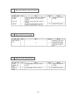
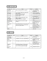
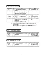
M -10 "54 MOTOR MALF" is displayed (The main motor rotation disabled )
Possible cause
Step
Check
Result
Remedy
Low-voltage
power supply
PCB
LV harness
Main PCB
1
Is the voltage of P7-1 in the main PCB
con24V?
No
Replace the main PCB
assy low-voltage power
supply PCB assy, or the
LV harness.
DC motor
harness
2
Does the voltage of P7-4 in the main PCB
connector drop from 5V to 0V after dropping
No
Replace the main PCB
assy.
DC motor assy
the voltage of P7-3 from 5V to 0V?
Yes
Replace the DC motor
harness or the DC motor
assy.
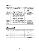
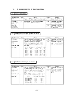
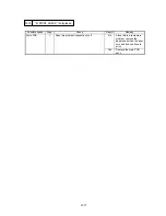
M-11 No paper pick-up from cassette (or MP tray)
Possible cause
Step
Check
Result
Remedy
Mis-operation
1
Is the paper feed mode set correctly?
No
Set paper feed mode
correctly.
Main PCB
2
Does the voltage of P3-20 (or 19) in the main
PCB connector rise from 0V to 5V and is a
pulses having about 11ms period generated at
P3-6, 7, 8 ,9 pin?
No
Replace the main PCB
assy.
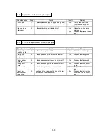
Feed flat cable
3
Does the voltage of P5-20 (or 19) in the paper
feeder PCB. Connector rise from 0V to 5V and
is the pulses having about 11ms period
generated at P3-6, 7, 8 ,9 pin?
No
Replace the feed flat
cable.
Paper feeder
PCB
4
Does the voltage of P3-1 (or P4-1) in the paper
feeder PCB connector drop from 24V to 0V
and is the chopping pulses generated at P1-1,
2, 5 ,6 pin?
No
Replace the Paper
feed/size-SW PCB assy.
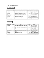
Pick-up(or MP
Pick) solenoid
5
Does the pick-up (or MP Pick) solenoid
operate?
No
Replace the pick-up (or
MP Pick) solenoid.
Paper feed
motor
6
Does the pick-up motor rotate?
No
Replace the paper feed
motor assy.
Summary of Contents for HL-2060
Page 1: ...MECHANICS ELECTRONICS SERVICE MANUAL LASER PRINTER ...
Page 41: ...III 8 A B F C D E 1 E 2 E 3 E 4 E 5 F Figure 3 7 Paper Feed Size SW PCB Circuit ...
Page 129: ...VII 16 Test for memory MEMORY DISPLAY MEMORY DEBUG MEMORY TEST exit MENU ...
Page 137: ...Appendix A 3 Main PCB Circuitry Diagram 1 7 CODE UK4058000 B512006 CIR 1 7 NAME A 3 ...
Page 138: ...Appendix A 4 Main PCB Circuitry Diagram 2 7 CODE UK4058000 B512006 CIR 2 7 NAME A 4 ...
Page 139: ...Appendix A 5 Main PCB Circuitry Diagram 3 7 CODE UK4058000 B512006 CIR 3 7 NAME A 5 ...
Page 140: ...Appendix A 6 Main PCB Circuitry Diagram 4 7 CODE UK4058000 B512006 CIR 4 7 NAME A 6 ...
Page 141: ...Appendix A 7 Main PCB Circuitry Diagram 5 7 CODE UK4058000 B512006 CIR 5 7 NAME A 7 ...
Page 142: ...Appendix A 8 Main PCB Circuitry Diagram 6 7 CODE UK4058000 B512006 CIR 6 7 NAME A 8 ...
Page 143: ...Appendix A 9 Main PCB Circuitry Diagram 7 7 CODE UK4058000 B512006 CIR 7 7 NAME A 9 ...
Page 144: ...Appendix A 10 Control Panel PCB Circuitry Diagram 1 1 CODE UK4077000 B512005 CIR NAME A 10 ...
Page 145: ...Appendix A 11 Laser LD PCB Circuitry Diagram 1 1 CODE UK3253000 B48K253 CIR NAME A 11 ...
Page 147: ...June 98 54T046NE0 HL2060 ...


