background image

4. Function explanations for each PCB   

4.1 PSDR board (POWER STAGE DRIVER) 


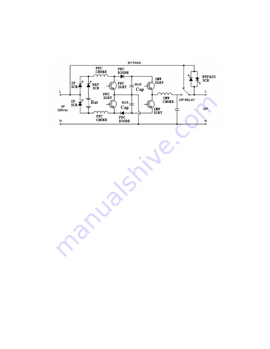
PSDR board configuration diagram 

4.1.1. The power stage (PSDR) consists of DC power supply, power factor correction, 

booster, inverter, and output circuits. DC power supply: The input of PSDR is 

connected to line input and b/-. So PSDR can provide DC power at line 
input and also at battery connected. DC power supply will provide 5V, 12V, ±15V

20V HFPW ± DC power for driver circuit. 

4.1.2.  Power factor correction: 

The DSP Controller make the input current and voltage in phase and therefore 

achieve a high input power factor. 

4.1.3. Booster: 

When the input AC power is on, the AC power goes through noise filter to the 

pre-charging circuit. The DC capacitors will be pre-charged. When the DC voltage 

on DC capacitor achieve the input AC power peak value then input SCR will turn 

on. After input SCR turn on, the charger will work and DC capacitors will have 1.4 

times of input RMS voltage. Turn on the KEY-ON display from bypass to online, DC 

capacitors will have 345VDC. 

4.1.4. Inverter sub-system: 

The UPS tra/- DC bus voltages to the AC output voltage through an 

inverter of half bridge configuration at normal operation. 

To construct a high frequency (19.2KHz) PWM inverter, the drivers receive 

switching signals from CPU PWM generation circuit through an IGBT Drive Board 

to trigger the upper IGBT and the lower IGBT alternately. The output of IGBT is 

filtered by a LC circuit to reduce the output voltage harmonic distortion.


Summary of Contents for 3T10KS

Page 1: ...to Bypass after 10min Load 130 Alarm and Transfer To Bypass after 1sec Overload Bypass mode 105 Load 130 Alarm Input Breaker May Trip Load 130 Alarm Input Breaker May trip and Cut Off Output after 1m...
Page 2: ...S voltage 345V 5V BUS voltage 345V 5V Difference between the BUS voltage absolute value 5V Balance voltage zero load 500mV Charging voltage 273V 1 If the above data exceed the electric specification r...

Page 3: ...3 2 Circuit block diagram Circuit block diagram the dashed indicates the charging board of the long backup time model and the real line indicates the charging board of the standard model...

Page 4: ...the MOSFET is off the primary stored energy 1 2Llp2 is delivered to the secondary to supply load current and replenish the charge on output capacitors that they had lost when the MOSFET was on This ci...

Page 5: ...l transfer to the battery mode If disconnecting the batteries from the UPS the UPS will transfer back to the line mode Press the ON button for 0 5 second when the UPS is in the battery mode the buzzer...

Page 6: ...d voltage of the input utility power will be in the same phase and the power factor is nearly 1 3 4 Inverter circuit Half bridge inverter topology The input of the half bridge inverter topology is DC...

Page 7: ...The INV mode the inverter output is supplied to the output terminals of the unit via the filter choke the inverter relay contact generally open closed when in INV mode and the load detecting transform...

Page 8: ...wer goes through noise filter to the pre charging circuit The DC capacitors will be pre charged When the DC voltage on DC capacitor achieve the input AC power peak value then input SCR will turn on Af...

Page 9: ...model The input of the charger is connected to REC When bypass breaker on and IP SCR on the charger will work The charge voltage is 273VDC and constant charge current is 4 2A Adjust the VR1 on charger...

Page 10: ...the output send to the rectifier on the PSDR board 4 7 CCB only for 3T15KS 3T20KS The CCB common control board is used to connect the PSDR board and the CNTL board It may help the CNTL board to contr...

Page 11: ...Note 1 indicates that the jumper is connected 0 indicates that nothing is connected For the pin plugs that are not listed here are not connected pin11 pin12 pin9 pin10 pin7 pin8 pin1 pin2 T6K 0 0 0 1...

Page 12: ...15 Over temperature Fault 08 Current Un share Fault 16 Inverter Short 09 Error Model 17 Communication Fault 10 SCI RX Error 18 Battery Open 11 Negative Output Power Fault 20 Inverter Relay Short 12 7...

Page 13: ...n you don t have a discharging resistor perform the maintenance after you have waited for at least 5 minutes and the BUS voltage is less than 10V Otherwise there may be electric shock 4 After you have...

Page 14: ...X is a digit from 0 to 6 then press the ENTER key output voltage will rise drop a little step 6 INV output voltage setting Type VXXX command XXX is 220 230 240 then press the ENTER key INV output vol...

Page 15: ...y UPS must be regulated 3 The UPS who have been replaced CNTL PSDR must be regulated again 4 All the commands use capital letters 5 All the above parameter regulation can not be accumulated 6 All the...

Page 16: ...e NTC on the CN107 of the PSDR board is damaged INV output short The Fault code is 09 The buzzer beeps continuously When the time that the INV output voltage keeps less than 50V and the output current...

Page 17: ...e output cable and ensure the length of cable is same Error Model The Fault code is 17 The UPS beeps continuously Ensure the model pin plugs in right position SCI RX Error The Fault code is 18 The UPS...

Page 18: ...normal IP Fuse Open The Warning code is 24 The buzzer beeps every second Check the IP fuse If the IP fuse is damaged replace the fuse immediately 7 5 PCB maintenance 1 Charger board 1 1 Charger board...

Page 19: ...R340 R339 R341 0 5 6 open 2 PSDR board 2 1 SCR part Item Checked components DVM Function Reference Value Fail Condition 1 F301 F302 0 open A K 1 4M short 2 Q301 Q302 G K 10 short 2 2 Boost part Item...

Page 20: ...8 Parallel maintenance This UPS has the function of parallel redundancy so if you need to add single UPS to the parallel system refer to the following operating process of adding a new UPS If you need...

Page 21: ...e slot of the parallel board and screw up the connector Screw the cover board of the parallel port back again 9 Close the input breakers of all of the UPSs including the new UPS in the parallel system...

Page 22: ...screw the cover board of the parallel port back again 6 Disassemble the cover board of the parallel port located on the UPS that need to be removed and remove the parallel cable and then screw the co...

Page 23: ...PORT I P L I P N KEY ON BAT BAT BAT BAT BAT BAT O P N GND GND L OTHUPS KEY OFF MAINT SWITCH G G G BYPASS O P EMI I P EMI I P TB O P TB PSDR CHARG PAREL PANEL CNTL REC CHGINPUT G K A G K A G K A E C G...

Page 24: ...T OTHUPS KEY OFF IP SCR MAINT SWITCH G O P EMI G G BYPASS I P EMI I P TB O P TB L3 L2 L1 PSDR CHARG PAREL PANEL CNTL REC CHGINPUT G K A G K A G K A E C G E C G G K A E C G G K A G K A G K A G K A G K...

Reviews: