background image

ADM1026

PRELIMINARY TECHNICAL DATA

– 2 0 –

REV. PrL

PRELIMINAR

Y

TECHNICAL

DA

TA

FAN INPUTS

Pins 3 to 6 and 9 to 12 may be configured as fan speed
measuring inputs by clearing the corresponding bit(s) of
Configuration Register 2 (address 01h) or as general-pur-
pose logic inputs/outputs by setting bits in this register.
The power-on default value for this register is 00h, which
means all the inputs are set for fan speed measurement.

Signal conditioning in the ADM1026 accommodates the
slow rise and fall times typical of fan tachometer outputs.
The maximum input signal range is 0 to +6.5V, even
where V

CC

 is less than 5V. In the event that these inputs

are supplied from fan outputs which exceed 0 to 6.5V, ei-
ther resistive attenuation of the fan signal or diode clamp-
ing must be included to keep inputs within an acceptable
range.

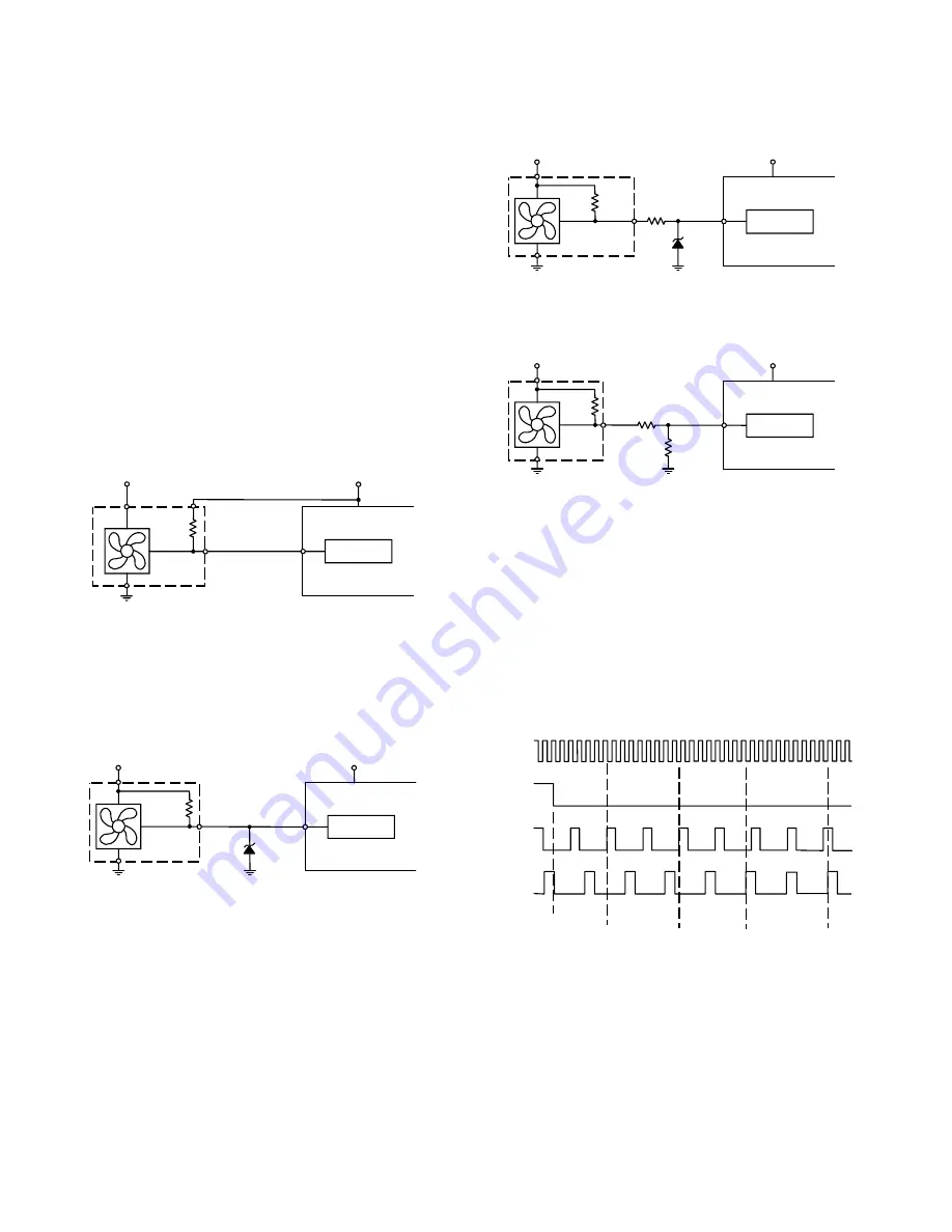
Figures 12a to 12d show circuits for most common fan
tacho outputs.

If the fan tacho output has a resistive pullup to V

CC

 then it can

be connected directly to the fan input, as shown in figure 12a.

+1 2 V

F A N  S P E E D

C O U N T E R

F AN (0-7)

P ULL UP

4.7k

T YP .

T A C H O

O U T P U T

V

C C

Figure 12a. Fan With Tach Pullup To +V

CC

.

If the fan output has a resistive pullup to +12V (or other
voltage greater than 6.5V) then the fan output can be
clamped with a zener diode, as shown in figure 12b. The
zener voltage should be chosen so that it is greater than
V

IH

 but less than 6.5V, allowing for the voltage tolerance

of the zener. A value of between 3V and 5V is suitable.

+1 2 V

F A N  S P E E D

C O U N T E R

F AN (0-7)

T A C H O

O U T P U T

Z D 1 *

Z E N E R

P ULL UP

4.7k

T YP .

*C HO O S E   Z D1  V O L T AG E   AP P RO X . 0 .8  x  V

C C

V

C C

Figure 12b. Fan with Tach. Pullup to Voltage >6.5V e.g.

12V) Clamped with Zener Diode

If the fan has a strong pullup (less than 1k

) to +12V, or

a totem-pole output, then a series resistor can be added to
limit the zener current, as shown in figure 11c. Alterna-
tively, a resistive attenuator may be used, as shown in fig-
ure 12d.

R1 and R2 should be chosen such that:

2V < V

PULLUP

 x R2/(R

PULLUP

 + R1 + R2) < 5V

The fan inputs have an input resistance of nominally
160k

 to ground, so this should be taken into account

when calculating resistor values.

With a pullup voltage of 12V and pullup resistor less than
1k

, suitable values for R1 and R2 would be 100k

 and

47k

.This will give a high input voltage of 3.83V.

+1 2 V

F A N  S P E E D

C O U N T E R

F AN (0-7)

P UL L UP

T Y P .  <1k

O R  T O T E M -P O L E

Z D 1

Z E N E R*

R1

10k

T A C H O

O /P

*C HO O S E  Z D1  V O L T AG E  AP P RO X .  0 .8  x V

C C

V

C C

Figure 12c. Fan with Strong Tach. Pullup to >V

CC

 or Totem-

Pole Output, Clamped with Zener and Resistor

+1 2 V

F A N  S P E E D

C O U N T E R

F AN (0-7)

T A C H O

O U T P U T

R 1 *

R 2 *

<1k

V

C C

*S E E  T E X T

Figure 12d. Fan with Strong Tach. Pullup to >V

CC

 or Totem-

Pole Output, Attenuated with R1/R2

FAN SPEED MEASUREMENT

The fan counter does not count the fan tacho output pulses
directly, because the fan speed may be less than 1000 RPM
and it would take several seconds to accumulate a reason-
ably large and accurate count. Instead, the period of the fan
revolution is measured by gating an on-chip 22.5kHz oscil-
lator into the input of an 8-bit counter for two periods of
the fan tacho output, as shown in Figure 13, so the accumu-
lated count is actually proportional to the fan tacho period
and inversely proportional to the fan speed.

22.5kHz

CLOCK

CONFIG

RE G. 1  BIT 0

FAN0

INP UT

FAN0

M E AS URE M E NT

P E RIO D

FAN1

M E AS URE M E NT

P E RIO D

S TART  O F

M ONITORING

CY CLE

FAN1

INP UT

1

2

3

4

1

2

3

4

Figure 13. Fan Speed Measurement

The monitoring cycle begins when a one is written to the
Monitor Bit (bit 0 of Configuration Register 1). The

INT

_Enable (Bit 1) should be set to one to enable the

INT

 output.

Speed measurement of the Fan 0 channel is initialized on
the first rising edge of the fan tach pulse after Start goes
low, and oscillator pulses are actually counted from the
second rising tach edge to the fourth rising edge. The
measurement then switches to Fan 1. Here again, the
measurement is initialized on the first tach pulse rising
edge after the Fan 0 measurement finishes and oscillator

Summary of Contents for ADM1026

Page 1: ...ut Reset Outputs Thermal Interrupt THERM Output Shutdown Mode to Minimize Power Consumption Limit Comparison of all Monitored Values APPLICATIONS Network Servers and Personal Computers Microprocessor...

Page 2: ...otherwise noted PRODUCT DESCRIPTION TheADM1026isacompletesystemhardwaremonitorformicroprocessor basedsystems providingmeasurementandlimitcomparisonofvarious systemparameters TheADM1026hasupto19analog...

Page 3: ...V IOUT 3 0mA VCC 2 85V 3 60V High Level Output Current IOH 0 1 100 A VOUT VCC SERIAL BUS DIGITAL INPUTS SCL SDA Input High Voltage VIH 2 2 V Input Low Voltage VIL 0 8 V Hysteresis 500 mV DIGITAL INPU...

Page 4: ...N0 GPIO0 FAN1 GPIO1 FAN2 GPIO2 FAN3 GPIO3 3 3V MAIN DGND FAN4 GPIO4 FAN5 GPIO5 FAN6 GPIO6 FAN7 GPIO7 S CL S DA AD D N TE S T O U T CI IN T P W M R E S ET S T B Y R E S ET M A IN AG N D 3 3V S T BY DA...

Page 5: ...ed as a general purpose digital I O pin This pin has an internal 10k pullup resistor 13 SCL Digital Input Open drain Serial Bus Clock Requires 2 2k pullup resistor 14 SDA Digital I O Serial Bus Data O...

Page 6: ...og Input Monitors processor core voltage 0 to 3 0V 34 AIN7 Analog Input General purpose 0 to 2 5V analog input 35 AIN6 Analog Input General purpose 0 to 2 5V analog input 36 AIN5 Analog Input General...

Page 7: ...f limit comparisons are stored in the Interrupt Status Registers and will generate an interrupt on the INT line pin 17 Any or all of the Interrupt Status Bits can be masked by appropriate programming...

Page 8: ...l operates as follows 1 The master initiates data transfer by establishing a START condition defined as a high to low transition on the serial data line SDA whilst the serial clock line SCL remains hi...

Page 9: ...and 3 at addresses 06h 0Ch and 13h EEPROM Registers 1 and 2 are for factory use only EEPROM Register 3 is used to set up the EEPROM op erating mode Setting bit 0 of EEPROM Register 3 puts the EEPROM...

Page 10: ...word protocol is used for four purposes The ADM1026 knows how to respond by the value of the command byte and EEPROM register 3 1 Write a single byte of data to RAM In this case the command byte is t...

Page 11: ...SMBus read protocols RECEIVE BYTE In this operation the master device receives a single byte from a slave device as follows 1 The master device asserts a start condition on SDA 2 The master sends the...

Page 12: ...put is measured 16 times and the measurements averaged to reduce noise so the total conversion time for each input is 11 38ms Measurements on the remote temperature D1 and D2 in puts take 2 13ms These...

Page 13: ...4 scale 01000000 l l l 8 000 8 063 6 750 6 678 3 330 3 560 2 220 2 237 2 000 2 016 1 500 1 512 1 500 1 512 1 250 1 260 128 1 2 scale 10000000 l l l 12 000 12 063 2 125 2 053 4 995 5 021 3 330 3 347 3...

Page 14: ...se The maximum negative voltage cor responds to zero output from the ADC This means that the upper and lower limits will be transposed 2 For the ADC output to be full scale when the negative voltage i...

Page 15: ...or diode connected tran sistor operated at a constant current exhibits a negative temperature coefficient of about 2mV o C Unfortunately the absolute value of Vbe varies from device to device and ind...

Page 16: ...racks on each side Provide a ground plane under the tracks if possible 3 Use wide tracks to minimize inductance and reduce noise pickup 10 mil track minimum width and spacing is recommended GND D D GN...

Page 17: ...ill form part of the input attenuators they will affect the accuracy of the analog measurement if their value is too high The analog input channels are cali brated assuming an external series resistor...

Page 18: ...LM 324 Figure 10c Fan Driver Circuit with Op Amp and P Channel MOSFET DAC 12V R1 100k R2 100k R3 3 9k R4 1k Q 3 IRF9620 Q1 Q2 M BT3904 DUA L Figure 10d Discrete Fan Drive Circuit with P Channel MOSFET...

Page 19: ...ss 04h and Fan Speed 2 Register address 05h set the minimum values for the DAC and PWM outputs Minimum DAC Code DACMIN 16 D DAC output voltage 2 5 Code 256 Minimum PWM Duty Cycle PWMMIN 6 67 D where D...

Page 20: ...as shown in fig ure 12d R1 and R2 should be chosen such that 2V VPULLUP x R2 RPULLUP R1 R2 5V The fan inputs have an input resistance of nominally 160k to ground so this should be taken into account...

Page 21: ...sters for the fans It should be noted that since fan period rather than speed is being measured a fan failure interrupt will occur when the measurement exceeds the limit value FAN MONITORING CYCLE TIM...

Page 22: ...Registers addresses 08h to OBh one of the GPIO Status Registers addresses 24h and 25h and one of the GPIO Mask Registers addresses 1Ch and 1Dh Setting a Direction Bit in one of the GPIO Configuration...

Page 23: ...UL T I P L E X E R 1 O UT OF LIMIT VALUE HIGH LIMIT MASK REGISTER 5 MASK REGISTER 6 STATUS REGISTER 6 GPIO0 TO GPIO7 GPIO8 TO GPIO15 STATUS REGISTER 5 MASKING DATA FROM SMBUS MASKING DATA FROM SMBUS S...

Page 24: ...UREMENT LOCAL TEMP MEASUREMENT START OF ANALOG MONITORING CYCLE INT INT CLEARED LOCAL TEM MEASUREMENT START OF ANALOG MONITORING CYCLE INT RE ASSERTED Figure 16 Delay After Clearing INT Before Re asse...

Page 25: ...mit a fixed hysteresis of 5o C is provided THERM will only be de asserted when the measured temperature of all three sensors is 5o C below the limit Whenever the THERM output changes INT will be as se...

Page 26: ...2 If any of the inputs shown in Figure 21 are unused they should not be connected direct to ground but via a resistor such as 10k This will allow the ATE Au tomatic Test Equipment to drive every inpu...

Page 27: ...the Fan Divisor Registers addresses 02h and 03h configuring the GPIO pins for input output polority us ing GPIO Configuration Registers 1 to 4 addresses 08h to 0Bh and bits 6 and 7 of Configuration R...

Page 28: ...de by setting bit 0 of the Configuration register to 0 This dis ables the internal ADC Full shutdown mode may then be achieved by setting bit 7 of the Test Register to 1 This turns off the analog outp...

Page 29: ...PRELIMINARY TECHNICAL DATA ADM1026 29 REV PrL PRELIMINARY TECHNICAL DATA AWAITING DIAGRAM AWAITING DIAGRAM AWAITING DIAGRAM AWAITING DIAGRAM AWAITING DIAGRAM Figure 27 ADM1026 Application Circuit...

Page 30: ...IO0 to GPIO3 as input or output and as active high or active low 09 GPIO Config 2 00h Configures GPIO4 to GPIO7 as input or output and as active high or active low 0A GPIO Config 3 00h Configures GPIO...

Page 31: ...ernal temp and supply voltage faults 21 Status Register 2 00h Interrupt status register for analog input faults 22 Status Register 3 00h Interrupt status register for fan faults 23 Status Register 4 0...

Page 32: ...VMAIN High Limit FFh High limit for analog VCC measurement 44 5V High Limit FFh High limit for 5V supply measurement 45 VCCP High Limit FFh High limit for processor core voltage measurement 46 12V Hig...

Page 33: ...o low limit 61 FAN1 High Limit FFh High limit for fan 1 speed measurement no low limit 62 FAN2 High Limit FFh High limit for fan 2 speed measurement no low limit 63 FAN3 High Limit FFh High limit for...

Page 34: ...ter 1 6 Enable PWM AFC 0 R W When this bit is 1 the PWM output is enabled for automatic fan speed control AFC based on temperature When this bit is 0 the PWM Output reflects the value in Reg 05h Fan S...

Page 35: ...rescaler division ratio for fan 4 speed measurement The division ratios oscillator frequencies and typical fan speeds based on 2 tach pulses per rev are as follows Code Divide by Osc Frequency kHz Fan...

Page 36: ...THERM 0 GPIO16 otherwise it is the THERM output 1 CI Clear 0 R W Writing a 1 to this bit will clear the CI latch This bit is self clearing 2 VREF Select 0 R W When this bit is 0 VREF pin 24 outputs 1...

Page 37: ...tion R W When this bit is 0 GPIO9 is configured as an input otherwise it is an output 3 GPIO9 Polarity R W When this bit is 0 GPIO9 is active low otherwise it is active high 4 GPIO10 Direction R W Whe...

Page 38: ...W This register contains the THERM limit for the TDM2 Temperature Channel Exceeding this limit will cause the THERM output pin to be asserted TABLE 23 REGISTER 10H INTERNAL TEMPERATURE TMIN POWER ON...

Page 39: ...e For the ADM1026 this nibble will read 4h TABLE 31 REGISTER 18H MASK REGISTER 1 POWER ON DEFAULT 00H Bit Name R W Description 0 Ext1 Temp Mask 0 R W When this bit is set interrupts generated on the E...

Page 40: ...ed on the AIN6 Voltage channel are masked out 7 AIN7 Mask 0 R W When this bit is set interrupts generated on the AIN7 Voltage channel are masked out TABLE 33 REGISTER 1AH MASK REGISTER 3 POWER ON DEFA...

Page 41: ...input are masked out 7 GPIO16 Mask 0 R W When this bit is set interrupts generated on the GPIO16 channel are masked out TABLE 35 REGISTER 1CH MASK REGISTER 5 POWER ON DEFAULT 00H Bit Name R W Descrip...

Page 42: ...7 GPIO15 Mask 0 R W When this bit is set interrupts generated on the GPIO15 channel are masked out TABLE 37 REGISTER 1EH INT TEMP OFFSET POWER ON DEFAULT 00H Bit Name R W Description 7 0 Int Temp Off...

Page 43: ...previous conversion cycle 0 otherwise 5 VCCP Status 0 R 1 if VCCP Value is above the High Limit or below the Low Limit on the previous conversion cycle 0 otherwise 6 12V Status 0 R 1 if 12V Value is a...

Page 44: ...as a result of Int temp readings exceeding the Int THERM limit This bit is also set once only if THERM mode is disengaged as a result of Int temp readings going 5C below Int THERM limit 1 VBAT Status...

Page 45: ...this bit asserts GPIO3 asserted may be active high or active low depending on setting of bit 7 in GPIO Configuration Register 1 4 GPIO4 Status 0 R When GPIO4 is configured as an input this bit is set...

Page 46: ...bit asserts GPIO11 asserted may be active high or active low depending on setting of bit 7 in GPIO Configuration Register 3 4 GPIO12 Status 0 R When GPIO12 is configured as an input this bit is set wh...

Page 47: ...his register contains the measured value of the DVCC analog input channel TABLE 50 REGISTER 2BH 3 3VMAIN MEASURED VALUE POWER ON DEFAULT 00H Bit Name R W Description 7 0 AVCC Value R This register con...

Page 48: ...he measured value of the AIN5 analog input channel TABLE 61 REGISTER 36H AIN6 MEASURED VALUE POWER ON DEFAULT 00H Bit Name R W Description 7 0 AIN6 Value R This register contains the measured value of...

Page 49: ...mp channel TABLE 72 REGISTER 41H EXT2 AIN9 HIGH LIMIT POWER ON DEFAULT 64H 100O C Bit Name R W Description 7 0 Ext2 Temp R W This register contains the high limit of the Ext2 Temp AIN9 AIN9 High Limit...

Page 50: ...Limit R W This register contains the low limit of the 3 3VMAIN analog input channel TABLE 82 REGISTER 4CH 5V LOW LIMIT POWER ON DEFAULT 00H Bit Name R W Description 7 0 5V Low Limit R W This register...

Page 51: ...ains the high limit of the AIN6 analog input channel TABLE 93 REGISTER 57H AIN7 HIGH LIMIT POWER ON DEFAULT FFH Bit Name R W Description 7 0 AIN7 High Limit R W This register contains the high limit o...

Page 52: ...gister contains the high limit of the FAN1 tach channel TABLE 104 REGISTER 62H FAN2 HIGH LIMIT POWER ON DEFAULT FFH Bit Name R W Description 7 0 FAN2 High Limit R W This register contains the high lim...

Page 53: ...scription 7 0 Ext1 Temp Offset R W This register contains the Offset Value for the External 1 Temperature Channel A 2 s complement number can be written to this register which is then added to the mea...

Page 54: ...INARY TECHNICAL DATA OUTLINE DIMENSIONS Dimensions shown in inches and mm 0o 7o 0 006 0 15 0 002 0 05 0 01 0 25 0o MIN 0 063 1 60 0 055 1 40 0 354 9 00 BSC 0 276 7 00 BSC 0 354 9 0 0 B S C 0 276 7 0 0...

Reviews: