ADM-SDEV-BASE/XCKU060 User Manual
V1.0 - 27th November 2018
3.3 Clocks
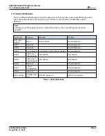
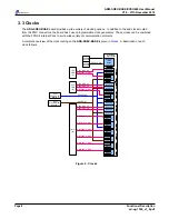
The ADA-SDEV-BASE board provides a wide variety of clocking options. In addition to the and clocks routed
from the FMC connectors, the board has 2 user-programmable clock generators. These clocks can be combined
with the FPGA's internal PLLs to suit a wide variety of communication protocols.
A complete overview of the clock routing on the ADA-SDEV-BASE is given in
Clocks
. A description of each
clock follows.
Ultrascale
MGT/ Banks
MGT228
REFCLK0
REFCLK1
MGT227
REFCLK0
REFCLK1
MGT226
REFCLK0
REFCLK1
MGT225
REFCLK0
REFCLK1
MGT224
REFCLK0
REFCLK1
MGT128
REFCLK0
REFCLK1
MGT127
REFCLK0
REFCLK1
User
Programmable
Source 0
MGT126
REFCLK0
REFCLK1
Bank 67
(DDR
Banks
66,67,68)
Bank 25
Bank 46
200MHz
Source
400MHz
Source
FABRIC_CLK
REFCLK_400
Bank 44
Bank 45
Bank 24
Bank 64
Bank 65
Bank 47
Bank 48
User
Programmable
Source 1
LPC
FMC
(J1)
CFG
FMC
(J2)
FMC+
(J3)
CLK1_M2C_0/1
PROGCLK0
PROGCLK1
GBTCLK1_0_M2C
CLK2_M2C_0/1
CLK2_M2C_2/3
GBTCLK2_0_M2C
CLK3_M2C_0/1
CLK3_M2C_2/3
GBTCLK3_3_M2C
GBTCLK3_4_M2C
GBTCLK3_5_M2C
GBTCLK3_0_M2C
GBTCLK3_1_M2C
GBTCLK3_2_M2C
Figure 5 : Clocks
Page 8
Functional Description
ad-ug-1360_v1_0.pdf


