background image

ADM-PCIE-8K5-FH User Manual
 

1 Introduction

The ADM-PCIE-8K5-FH is a high-performance reconfigurable computing card intended for Data Center

applications, featuring a Xilinx Kintex UltraScale FPGA.

Figure 1 : ADM-PCIE-8K5-FH Product Photo

1.1 Key Features

Key Features

PCIe Gen1/2/3 x1/2/4/8 capable

Half-length, full-height x8 PCIe form factor

Two banks of DDR4 SDRAM 72 bit wide memory (ECC), 16GB (8GB per bank) default rated at 2400MT/s,
32GB option rated at 1866MT/s.

Four SFP+ sites capable of data rates up to 16.375 Gbps per channel

Optional Samtec FireFly sites capable of data rates up to 16.375 Gbps per channel (65.5 Gbps per
module). Can be routed to front panel or adjacent card slots.

Optional SMA/U.FL timing input

Front Panel JTAG Access via USB port

FPGA configurable over USB/JTAG and BPI configuration flash

XCKU115-2FLVA1517I Or XCKU060-2FLVA1517I FPGA

Voltage, current, and temperature monitoring

All components rated for operation down to -40 DegC

1.2 Order Code

ADM-PCIE-8K5-FH(d)(m)(c)(a)(o)(f)(NF)

See http://www.alpha-data.com/pdfs/adm-pcie-8k5-fh.pdf for complete ordering options.

Page 1

Introduction
ad-ug-1342_v1_0.pdf

Summary of Contents for ADM-PCIE-8K5-FH

Page 1: ...ADM PCIE 8K5 FH User Manual Document Revision 1 0 16th Feb 2018...

Page 2: ...without prior written consent from Alpha Data Parallel Systems Ltd Head Office Address 4 West Silvermills Lane Edinburgh EH3 5BD UK Telephone 44 131 558 2600 Fax 44 131 558 2700 email sales alpha dat...

Page 3: ...PCI Express 9 3 4 DDR4 SDRAM 10 3 4 1 MIG IP setup requirements rev2 newer PCBs 10 3 5 SFP 11 3 6 FireFly 12 3 7 System Monitor 13 3 7 1 Automatic Temperature Monitoring 13 3 7 2 System Monitor Statu...

Page 4: ...Table 13 Status LED Definitions 14 Table 14 Complete Pinout Table 21 List of Figures Figure 1 ADM PCIE 8K5 FH Product Photo 1 Figure 2 Thermal Performance 3 Figure 3 8K5 FH With Attached Optional Blo...

Page 5: ...Four SFP sites capable of data rates up to 16 375 Gbps per channel Optional Samtec FireFly sites capable of data rates up to 16 375 Gbps per channel 65 5 Gbps per module Can be routed to front panel...

Page 6: ...5 FH is shipped with a full height PCIe card bracket installed by default 2 2 3 Power Requirements The PCIe Specification permits a standard full height half length PCIe card to dissipate a maximum 75...

Page 7: ...ature to your system ambient and select User Override for the Effective theta JA and enter the figure associated with your system LFM in the blank field Proceed to enter all applicable design elements...

Page 8: ...general purpose use clocking control pins debug etc and low speed serial communications and a robust system monitor Depending on selected FPGA XCKU115 only two optional Samtec FireFly connectors may...

Page 9: ...F State ON State SW1 1 OFF User Switch Pin AV18 1 Pin AV18 0 SW1 2 OFF Flash Lockdown Flash block Lockdown enabled Flash block Lockdown disabled SW1 3 OFF Service Mode Regular Operation Firmware updat...

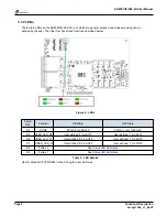
Page 10: ...F State D4 DONE FPGA is configured FPGA is not configured D2 USER_LED_G0 User defined 0 pin AT19 User defined 1 pin AT19 D8 USER_LED_G1 User defined 0 pin AU19 User defined 1 pin AU19 D7 USER_LED_R Us...

Page 11: ...Factory Default MGTREFCLK0_228 NB6L11S Fanout Memory Interface Clock 300Mhz IO Bank 66 Memory Interface Clock 300Mhz IO Bank 44 FABRIC_CLK 200MHz IO Bank 64 200MHz 30ppm Source EMCCLK 100MHz IO Bank...

Page 12: ...ence Clocks The SFP cages are also located such that they can be clocked from a Si5328 jitter attenuator clock multiplier If jitter attenuation is required please see the reference documentation for t...

Page 13: ...d P pin N pin MEM_CLK_0 IO_L11_T1U_GC_66 DIFF_HSTL_I_12 or SSTL G16 G15 MEM_CLK_1 IO_L11_T1U_GC_44 DIFF_HSTL_I_12 or SSTL AM22 AN22 Table 10 Memory Reference Clocks 3 3 PCI Express The ADM PCIE 8K5 FH...

Page 14: ...ater An example project with traffic generator is available with purchase of the ADM PCIE 8K5 SDK However all the information required to generate a complete MIG IP core is available within this user...

Page 15: ...it Ethernet or any other protocol supported by the Xilinx GTH Transceivers Please see Xilinx User Guide UG576 for more details on the capabilities of the transceivers Both SFP cages have control signa...

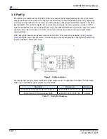
Page 16: ...ion on FireFly can be found at https www samtec com optics optical cable mid board firefly Both FireFly sites have control signals connected to the FPGA Their connectivity is detailed in the Complete...

Page 17: ...ion ADC00 12 0V Board Input Supply ADC01 3 3V Board Input Supply ADC02 3 3V Board Input Auxilary Power Supply ADC03 3 3V Internally generated supply ADC04 2 5V Clock Voltage Supply ADC05 1 8V FPGA IO...

Page 18: ...dby Powered off Flashing Green Flashing Red together Attention critical alarm active Flashing Green Flashing Red alternating Service Mode Flashing Green Red Attention alarm active Red Missing applicat...

Page 19: ...PGA For convenience the FPGA can be configured directly from the lower USB connection on the front panel The ADM PCIE 8K5 FH utilizes the Digilent USB JTAG converter box which is supported by the Xili...

Page 20: ...ata recommends that region 0 is used as a fallback image this permits relatively simple recovery without requiring direct programming of the FPGA over the front panel USB connection in the event of pr...

Page 21: ...lash Write Interface Alpha Data s reference design bridge allows users to write images to the BPI configuration flash over the PCIE interface Other customers may want similar functionality built into...

Page 22: ...in the design The direct connect GP0 signals are limited to 1 8V by a quickswitch 74CBTLVD3861BQ in order to protect the FPGA from overvoltage on IO pins This quickswitch allows the signals to travel...

Page 23: ...2 RMC6TG The address pins A2 A1 and A0 are all strapped to a logical 0 Write protect WP Serial Clock SCL and Serial Data SDA pin assignments can be found in Complete Pinout Table with the names SPARE_...

Page 24: ...ADM PCIE 8K5 FH User Manual Page Intentionally left blank Page 20 Functional Description ad ug 1342_v1_0 pdf...

Page 25: ..._A11 1 2 B14 DDR4_0_A12 1 2 J15 DDR4_0_A13 1 2 H12 DDR4_0_A14 1 2 B16 DDR4_0_A15 1 2 A15 DDR4_0_A16 1 2 L13 DDR4_0_A17 1 2 G12 DDR4_0_A2 1 2 E13 DDR4_0_A3 1 2 A13 DDR4_0_A4 1 2 C12 DDR4_0_A5 1 2 B12 D...

Page 26: ...7 1 2 P13 DDR4_0_DM8 1 2 B20 DDR4_0_DQ0 1 2 C18 DDR4_0_DQ1 1 2 A24 DDR4_0_DQ10 1 2 B24 DDR4_0_DQ11 1 2 B21 DDR4_0_DQ12 1 2 C23 DDR4_0_DQ13 1 2 D21 DDR4_0_DQ14 1 2 A22 DDR4_0_DQ15 1 2 J19 DDR4_0_DQ16 1...

Page 27: ...0_DQ39 1 2 A20 DDR4_0_DQ4 1 2 G22 DDR4_0_DQ40 1 2 E23 DDR4_0_DQ41 1 2 G21 DDR4_0_DQ42 1 2 F23 DDR4_0_DQ43 1 2 H24 DDR4_0_DQ44 1 2 E22 DDR4_0_DQ45 1 2 H23 DDR4_0_DQ46 1 2 E21 DDR4_0_DQ47 1 2 J23 DDR4_0...

Page 28: ..._0_DQ71 1 2 C21 DDR4_0_DQ8 1 2 D23 DDR4_0_DQ9 1 2 B17 DDR4_0_DQS0_C 1 2 C17 DDR4_0_DQS0_T 1 2 B22 DDR4_0_DQS1_C 1 2 C22 DDR4_0_DQS1_T 1 2 J16 DDR4_0_DQS2_C 1 2 K16 DDR4_0_DQS2_T 1 2 N22 DDR4_0_DQS3_C...

Page 29: ...1_A17 1 2 AL20 DDR4_1_A2 1 2 AJ23 DDR4_1_A3 1 2 AK21 DDR4_1_A4 1 2 AM20 DDR4_1_A5 1 2 AN21 DDR4_1_A6 1 2 AD21 DDR4_1_A7 1 2 AG21 DDR4_1_A8 1 2 AP20 DDR4_1_A9 1 2 AR23 DDR4_1_ACT_N 1 2 AJ20 DDR4_1_ALER...

Page 30: ...AV26 DDR4_1_DQ13 1 2 AT28 DDR4_1_DQ14 1 2 AW26 DDR4_1_DQ15 1 2 AL28 DDR4_1_DQ16 1 2 AJ25 DDR4_1_DQ17 1 2 AH26 DDR4_1_DQ18 1 2 AH24 DDR4_1_DQ19 1 2 AT24 DDR4_1_DQ2 1 2 AJ26 DDR4_1_DQ20 1 2 AJ24 DDR4_1_...

Page 31: ...R4_1_DQ44 1 2 H39 DDR4_1_DQ45 1 2 G34 DDR4_1_DQ46 1 2 G36 DDR4_1_DQ47 1 2 J38 DDR4_1_DQ48 1 2 J35 DDR4_1_DQ49 1 2 AU22 DDR4_1_DQ5 1 2 K37 DDR4_1_DQ50 1 2 K35 DDR4_1_DQ51 1 2 J39 DDR4_1_DQ52 1 2 J34 DD...

Page 32: ...25 DDR4_1_DQS1_T 1 2 AL25 DDR4_1_DQS2_C 1 2 AL24 DDR4_1_DQS2_T 1 2 AG24 DDR4_1_DQS3_C 1 2 AF24 DDR4_1_DQS3_T 1 2 AR25 DDR4_1_DQS4_C 1 2 AP25 DDR4_1_DQS4_T 1 2 H38 DDR4_1_DQS5_C 1 2 H37 DDR4_1_DQS5_T 1...

Page 33: ...RX1_N MGT G4 FIREFLY0_RX1_P MGT F1 FIREFLY0_RX2_N MGT F2 FIREFLY0_RX2_P MGT E3 FIREFLY0_RX3_N MGT E4 FIREFLY0_RX3_P MGT AP19 FIREFLY0_SCL 3 3 AK18 FIREFLY0_SDA 3 3 AK17 FIREFLY0_SEL_L 3 3 H5 FIREFLY0_...

Page 34: ...X1_N MGT C8 FIREFLY1_TX1_P MGT B5 FIREFLY1_TX2_N MGT B6 FIREFLY1_TX2_P MGT A7 FIREFLY1_TX3_N MGT A8 FIREFLY1_TX3_P MGT AJ15 FLASH_A0 1 8 AK15 FLASH_A1 1 8 AN13 FLASH_A10 1 8 AN12 FLASH_A11 1 8 AP14 FL...

Page 35: ...FLASH_DQ11 1 8 AK13 FLASH_DQ12 1 8 AK12 FLASH_DQ13 1 8 AH13 FLASH_DQ14 1 8 AJ13 FLASH_DQ15 1 8 AC9 FLASH_DQ2 1 8 AD9 FLASH_DQ3 1 8 AF14 FLASH_DQ4 1 8 AG14 FLASH_DQ5 1 8 AE13 FLASH_DQ6 1 8 AF13 FLASH_D...

Page 36: ...ded AM22 MEM_CLK_1_PIN_P 1 2 External Term Provided H9 PCIE_REFCLK_1_PIN_N MGT_CLK H10 PCIE_REFCLK_1_PIN_P MGT_CLK AT9 PCIE_REFCLK_2_PIN_N MGT_CLK AT10 PCIE_REFCLK_2_PIN_P MGT_CLK AW3 PCIE_RX0_N MGT A...

Page 37: ...PCIE_TX7_PIN_N MGT AM6 PCIE_TX7_PIN_P MGT AE15 PERST_1V8_0_L 1 8 AM15 PERST_1V8_1_L 1 8 AU31 POWER9_SCL_1V8 1 8 AV31 POWER9_SDA_1V8 1 8 AL30 PPS_BUF_1V8 1 8 AA9 PROGRAM_B_1V8 1 8 P11 PUDC_B 1 8 AH28...

Page 38: ...DA 3 3 AF17 SFP 2_MOD_ABS 3 3 AF19 SFP 2_SCL 3 3 AE17 SFP 2_SDA 3 3 AN17 SFP 3_MOD_ABS 3 3 AG19 SFP 3_SCL 3 3 AD18 SFP 3_SDA 3 3 AU30 SI5328_1V8_SCL 1 8 AU29 SI5328_1V8_SDA 1 8 AN32 SI5328_REFCLK_IN_N...

Page 39: ...r Manual Pin Number Signal Name Bank Voltage AJ29 TE485 1 8 AT19 USER_LED_G0 3 3 AU19 USER_LED_G1 3 3 AU20 USER_LED_R 3 3 AV18 USR_SW 3 3 Table 14 Complete Pinout Table Page 35 Complete Pinout Table a...

Page 40: ...e Address 4 West Silvermills Lane Edinburgh EH3 5BD UK Telephone 44 131 558 2600 Fax 44 131 558 2700 email sales alpha data com website http www alpha data com Address 611 Corporate Circle Suite H Gol...

Reviews: