ADM-PCIE-8K5-FH User Manual
3.1.1 Switches
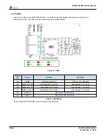
The ADM-PCIE-8K5-FH has a quad DIP switch SW1, located on the rear side of the board. The function of each
switch in SW1 is detailed below:
Figure 5 : Switches
Switch
Factory
Default
Function
OFF State
ON State
SW1-1
OFF
User
Switch
Pin AV18 = '1'
Pin AV18 = '0'
SW1-2
OFF
Flash
Lockdown
Flash block Lockdown enabled
Flash block Lockdown disabled
SW1-3
OFF
Service
Mode
Regular Operation
Firmware update service mode
SW1-4
OFF
PCIe Edge
JTAG
JTAG to FPGA from USB
JTAG to FPGA from PCIe Edge
Table 3 : SW1 Switch Functions
Use IO Standard "LVCMOS33" when constraining the user switch pin.
Page 5
Functional Description
ad-ug-1342_v1_0.pdf


