ADM-PCIE-8K5-FH User Manual
3.11 GPIO Option
The ADM-PCIE-8K5-FH has an optional GPIO feature. This feature is not fit by default and must be specified in
the part number. See
Order Code
for more details on ordering options.
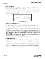
The GPIO option consists of a versatile shrouded connector from Molex with part number 0878331220 that give
users with custom IO requirements multiple connectivity options. The connector houses two types of signal,
direct connect to FPGA signals and low speed serial communication signals.
Recommended mating plug: Molex 0875681273
Figure 13 : GPIO Connector
3.11.1 Direct Connect FPGA Signals
Four nets are broken out to the GPIO header as two differential pairs. The first pair, is called GP0 and these
signal are suitable for any 1.8V supported signaling standards supported by the Xilinx UltraScale architecture.
See Xilinx UG571 for IO options. LVDS and 1.8 CMOS are popular options. The second pair is EXT_CLK, which
is a differential pair that is routed directly to a GTH clock input. This can be used to either clock the FireFly GTH
tiles, or as a global clock used anywhere in the design.
The direct connect GP0 signals are limited to 1.8V by a quickswitch (74CBTLVD3861BQ) in order to protect the
FPGA from overvoltage on IO pins. This quickswitch allows the signals to travel in either direction with only 4
ohms of series impedance and less than 1ns of propagation delay. The nets are directly connected to the FPGA
after the quickswitch.
Direct connect signal names are labeled GP0_1V8_P/N and EXT_CLK_P/N to show polarity and grouping. The
signal pin allocations can be found in
Complete Pinout Table
This header is always populated on the board and these signal are always available.
3.11.2 Low Speed Serial IO
A pin configurable serial buffer transceiver allows for RS232, RS485, and RS422 signal standard support. For
details on configuring the transceiver please reference the IC manufacturer datasheet. Linear Technologies part
number LTC2870. Direct link: http://cds.linear.com/docs/en/datasheet/28701fa.pdf
Signal naming is kept consistent with the Linear Tech datasheet and FPGA pin allocations can be found in the
Complete Pinout Table
. Be sure to constrain and drive each control pin for expected behavior.
This device is not normally fitted. Please see the order options if you require RS232/485 signaling standards.
Page 18
Functional Description
ad-ug-1342_v1_0.pdf


