background image

Figure 6-9.  Power Transformer Wiring Diagram for Models 655xA and 665xA (Sheet 2 of 3)

166   Diagrams

Summary of Contents for 6541A

Page 1: ...nd above Agilent Model 6555A US36340101 and above Agilent Model 6641A US36410101 and above Agilent Model 6642A US36400101 and above Agilent Model 6643A US36400101 and above Agilent Model 6644A US36410101 and above Agilent Model 6645A US36390101 and above Agilent Model 6651A US36400101 and above Agilent Model 6652A US36400101 and above Agilent Model 6653A US36400101 and above Agilent Model 6654A US...

Page 2: ...ed to Customer from another country Agilent Technologies Inc shall pay for return of products to Customer Warranty services outside the country of initial purchase are included in Agilent Technologies Inc s product price only if Customer pays Agilent Technologies Inc international prices defined as destination local currency price or U S or Geneva Export price If Agilent Technologies Inc is unable...

Page 3: ...al blow time delay etc should be used Do not use repaired fuses or short circuited fuseholders To do so could cause a shock or fire hazard Do not operate this instrument in the presence of flammable gases or fumes Do not install substitute parts or perform any unauthorized modification to this instrument Some procedures described in this manual are performed with power supplied to the instrument w...

Page 4: ...lectrician install an external switch Notice The information contained in this document is subject to change without notice Agilent Technologies makes no warranty of any kind with regard to this material including but not limited to the implied warranties of merchantability and fitness for a particular purpose Agilent Technologies shall not be liable for errors contained herein or for incidental o...

Page 5: ...D 14 Transient Recovery Time 15 Constant Current CC Tests 15 CC Setup 15 Current Programming and Readback Accuracy 15 Current Sink CC Operation 16 CC Load and Line Regulation 16 CC Load Effect 16 CC Source Effect 17 CC Noise PARD 17 Troubleshooting 31 Introduction 31 Test Equipment Required 31 Overall Troubleshooting 34 Power On Self Test 34 Signature Analysis 35 Firmware Revisions for Models 664x...

Page 6: ...placement 78 Principles of Operation 81 Introduction 81 I O INTERFACE SIGNALS 81 Overall Block Diagram Figure 4 2 83 Detailed Block Diagram Discussion 83 Secondary Interface Circuits Figure 4 3 83 Output Power and Control Circuits Figure 4 4 86 Output Power 86 Control Circuits 86 A3 Front Panel Board Circuits Figure 4 5 89 A2 GPIB Board Circuits For Agilent Models 664xA and 665xA Only 90 Isolator ...

Page 7: ...ed In Text 1 Power supply models can be divided into 200 watt and 500 watt models A 4 in the third position of the model number indicates a 200 watt supply while the digit 5 in the third position indicates a 500 watt unit 2 In addition power supplies can be divided according to GPIB supplies or Analog Programmable supplies All GPIB models have a 6 in the second position of the model number while A...

Page 8: ...pply chassis at the output terminals and at the programming terminals Firmware Revisions The supply s firmware resides in the front panel board s ROM chip A3U4 and in the main board s microprocessor chip AlU504 For models 664xA and 665xA firmware also resides in the GPIB board ROM chip A2U106 For GPIB models 664xA and 665xA you can use the IDN query as described in Chapter 3 to get the firmware re...

Page 9: ...f the supply fails the self test refer to the overall troubleshooting procedures in Chapter 3 of this manual If any failures are encountered or if abnormal test results are observed refer to the Troubleshooting Procedures in Chapter 3 of this manual The troubleshooting procedures will determine if repair and or calibration is required Calibration procedures are given in Appendix A of the appropria...

Page 10: ... range must exceed range of supply under test Power range 250 W minimum Agilent N3300A mainframe with Agilent N3306A 60 V plug in module or Agilent N3305A 150 V plug in module GPIB Controller1 Full GPIB capabilities Agilent 82350B Load Resistor 0 1 Ω 5 300 W for Agilent 6541A 6641A 6551A 6651A 6552A 6652A models Ohmite C300KRlO l 0 Ω 5 300 W for Agilent 6542A 6543A 6544A 6545A 6553A 6554A 6555A 66...

Page 11: ...ly may have to be taken into account Wait statements can be used in the test program if the test system is faster than the supply Current Monitoring Resistor To eliminate output current measurement error caused by voltage drops in the leads and connections connect the current monitoring resistor between the OUT and the load as a four terminal device Connect the current monitoring leads inside the ...

Page 12: ...12 Verification Figure 2 1 Basic Test Setup CV TESTS CV TESTS ...

Page 13: ...n off the supply and connect a digital voltmeter between the S and the S terminals as shown in Figure 2 1 b Turn on the supply and program the supply to zero volts and the maximum programmable current see Table 2 3 with the load off c Record the output voltage readings on the digital voltmeter DVM and the front panel display The readings should be within the limits specified in the performance tes...

Page 14: ... the front panel display The CV annunciator on the front panel must be on If it is not adjust the load so that the output current drops slightly e Adjust the transformer to 13 below the nominal line voltage e g l04 4 Vac for a 120 Vac nominal line voltage input f Record the output voltage reading on the DVM g Adjust the transformer to 6 above the nominal line voltage e g 127 2 Vac for 120 Vac nomi...

Page 15: ...s Check both loading and unloading transients by triggering on the positive and negative slope Figure 2 2 Transient Response Wavetorm Constant Current CC Tests CC Setup Follow the general setup instructions in the Measurement Techniques paragraph and the specific instructions given in the following paragraphs Current Programming and Readback Accuracy This test verifies that the current programming...

Page 16: ...e model under CURRENT SINK DISPLAY AND READBACK CC Load and Line Regulation These tests CC Load Effect and CC Source Effect given below are tests of the DC regulation of the power supply s output current To insure that the values read are not the instantaneous measurement of the AC peaks of the output current ripple several DC measurements should be made and the average of these reading calculated...

Page 17: ... that the CC annunciator is on If it is not adjust the load so that the output voltage drops slightly e Adjust the transformer to 13 below the nominal line voltage f Record the output current reading DVM reading current monitoring resistor in ohms g Adjust the transformer to 6 above the nominal line voltage h Record the output current reading again The difference in the current readings in steps f...

Page 18: ...18 Verification Figure 2 3 CC RMS Noise Measurement Test Setup ...

Page 19: ...________________________________________________________________________________________ ____________________________________________________________________________________________ ____________________________________________________________________________________________ ____________________________________________________________________________________________ ________________________________...

Page 20: ...V _______mV Vout 1 mV Source Effect Vout 0 5 mV _______mV Vout 0 5 mV PARD Ripple and Noise Peak to Peak RMS 0 0 _______mV _______µV 3 mV 300 µV Transient Response Time at 100 µs 0 _______mV 20 mV Constant Current Tests Current Programming and Readback Low Current 0 A Iout Front Panel Display Readback 26 mA Iout 18 mA _______mA _______mA 26 mA Iout 18 mA High Current 20 A Iout Front Panel Display ...

Page 21: ...___mV Vout 2 mV Source Effect Vout 0 5 mV _______mV Vout 0 5 mV PARD Ripple and Noise Peak to Peak RMS 0 0 _______mV _______µV 3 mV 300 µV Transient Response Time at 100 µs 0 _______mV 20 mV Constant Current Tests Current Programming and Readback Low Current 0 A Iout Front Panel Display Readback 13 mA Iout 9 1 mA _______mA _______mA 13 mA Iout 9 1 mA High Current 10 A Iout Front Panel Display Read...

Page 22: ..._____mV Vout 3 mV Source Effect Vout 1 mV _______mV Vout 1 mV PARD Ripple and Noise Peak to Peak RMS 0 0 _______mV _______µV 4 mV 400 µV Transient Response Time at 100 µs 0 _______mV 35 mV Constant Current Tests Current Programming and Readback Low Current 0 A Iout Front Panel Display Readback 6 7 mA Iout 5 mA _______mA _______mA 6 7 mA Iout 5 mA High Current 6 A Iout Front Panel Display Readback ...

Page 23: ... Vout 4 mV Source Effect Vout 1 mV _______mV Vout 1 mV PARD Ripple and Noise Peak to Peak RMS 0 0 _______mV _______µV 5 mV 500 µV Transient Response Time at 100 µs 0 _______mV 60 mV Constant Current Tests Current Programming and Readback Low Current 0 A Iout Front Panel Display Readback 4 1 mA Iout 3 mA _______mA _______mA 4 1 mA Iout 3 mA High Current 3 5 A Iout Front Panel Display Readback 3 490...

Page 24: ...V Vout 5 mV Source Effect Vout 2 mV _______mV Vout 2 mV PARD Ripple and Noise Peak to Peak RMS 0 0 _______mV _______µV 7 mV 700 µV Transient Response Time at 100 µs 0 _______mV 120 mV Constant Current Tests Current Programming and Readback Low Current 0 A Iout Front Panel Display Readback 1 7 mA Iout 1 3 mA _______mA _______mA 1 7 mA Iout 1 3 mA High Current 1 5 A Iout Front Panel Display Readback...

Page 25: ...______mV Vout 1 mV Source Effect Vout 0 5 mV _______mV Vout 0 5 mV PARD Ripple and Noise Peak to Peak RMS 0 0 _______mV _______µV 3 mV 300 µV Transient Response Time at 100 µs 0 _______mV 20 mV Constant Current Tests Current Programming and Readback Low Current 0 A Iout Front Panel Display Readback 60 mA Iout 67 mA _______mA _______mA 60 mA Iout 67 mA High Current 50 A Iout Front Panel Display Rea...

Page 26: ..._____mV Vout 2 mV Source Effect Vout 0 5 mV _______mV Vout 0 5 mV PARD Ripple and Noise Peak to Peak RMS 0 0 _______mV _______µV 3 mV 300 µV Transient Response Time at 100 µs 0 _______mV 20 mV Constant Current Tests Current Programming and Readback Low Current 0 A Iout Front Panel Display Readback 25 mA Iout 26 mA _______mA _______mA 25 mA Iout 26 mA High Current 25 A Iout Front Panel Display Read...

Page 27: ...____mV Vout 3 mV Source Effect Vout 1 mV _______mV Vout 1 mV PARD Ripple and Noise Peak to Peak RMS 0 0 _______mV _______µV 4 mV 400 µV Transient Response Time at 100 µs 0 _______mV 35 mV Constant Current Tests Current Programming and Readback Low Current 0 A Iout Front Panel Display Readback 13 mA Iout 15 mA _______mA _______mA 13 mA Iout 15 mA High Current 15 A Iout Front Panel Display Readback ...

Page 28: ...______mV Vout 4 mV Source Effect Vout 1 mV _______mV Vout 1 mV PARD Ripple and Noise Peak to Peak RMS 0 0 _______mV _______µV 5 mV 500 µV Transient Response Time at 100 µs 0 _______mV 60 mV Constant Current Tests Current Programming and Readback Low Current 0 A Iout Front Panel Display Readback 8 mA Iout 7 mA _______mA _______mA 8 mA Iout 7 mA High Current 9 A Iout Front Panel Display Readback 8 9...

Page 29: ...5 mV _______mV Vout 5 mV Source Effect Vout 2 mV _______mV Vout 2 mV PARD Ripple and Noise Peak to Peak RMS 0 0 _______mV _______µV 7 mV 700 µV Transient Response Time at 100 µs 0 _______mV 120 mV Constant Current Tests Current Programming and Readback Low Current 0 A Iout Front Panel Display Readback 4 mA Iout 3 mA _______mA _______mA 4 mA Iout 3 mA High Current 4 A Iout Front Panel Display Readb...

Page 30: ......

Page 31: ...cuit Figure 3 1 shows the location of the circuit boards and other chassis mounted components within the power supply Once a problem has been isolated to a circuit board additional troubleshooting procedures are available to isolate the problem to the defective component s Disassembly procedures are provided at the end of this chapter and should be referred to as required in order to gain access t...

Page 32: ...32 Troubleshooting Figure 3 1 Top View with Cover Removed for 655xA 665xA Models Sheet 1 of 2 ...

Page 33: ...Troubleshooting 33 Figure 3 1 Top View with Cover Removed for 655xA 665xA Models Sheet 2 of 2 ...

Page 34: ...the supply fails any of the tests you are directed to the applicable troubleshooting procedure or flow chart Signature analysis SA is used to troubleshoot some of the supply s digital circuits Power On Self Test The power on self test sequence consists of tests of the front panel primary GPIB interface for 664xA 665xA Models only secondary interface circuits and the isolator board for 654xA 655xA ...

Page 35: ... tests are given in Table 3 3 SA tests for the front panel are given in Table 3 4 and the secondary interface SA tests are given in Table 3 5 References are made to the appropriate SA table from the troubleshooting flow charts or procedures The following general rules apply to signature analysis testing 1 Be sure to use the correct test setup connections for the specific test 2 Note the signatures...

Page 36: ...ctive E9 SEC ROM Secondary interface ROM test failed power on and for models 664xA 665xA also TST Microprocessor AlU504 defective El0 SEC 5 V Secondary interface 5 volt read back test failed power on and for models 664xA 665xA also TST Comparators AlU513 read back DAC AlU511 U512 or secondary bias supply defective E11 TEMP Ambient temperature read back test failed power on and for models 664xA 665...

Page 37: ...Troubleshooting 37 Figure 3 2 Overall Troubleshooting Flow Diagram Sheet 1 of 4 ...

Page 38: ...38 Troubleshooting Figure 3 2 Overall Troubleshooting Flow Diagram Sheet 2 of 4 ...

Page 39: ...Troubleshooting 39 Figure 3 2 Overall Troubleshooting Flow Diagram Sheet 3 of 4 ...

Page 40: ...40 Troubleshooting Figure 3 2 Overall Troubleshooting Flow Diagram Sheet 4 of 4 ...

Page 41: ...OGIES 6651A 0 fA 01 05sA 01 02pA 01 05 where pA 01 05 is the primary interface p firmware revision see Table 3 3 fA 01 05 is the front panel f firmware revision see Table 3 4 sA 01 02 is the secondary interface s firmware revision see Table 3 5 For Agilent models 654xA 655xA the revision level of the ROMs can be found on the label affixed to the physical IC chip itself Test Headers For Agilent mod...

Page 42: ...ST REPAIR CALIBRATION discussion later in this chapter 7 and 8 NORM This is the normal operating storage position for the jumper Primary Interface Test Connector A2J106 Pins For Agilent Models 664xA 665xA Only Description 1 and 2 SA MODE With these pins jumpered the primary interface is placed in the SA mode Removing this jumper takes the primary interface out of the SA mode 3 and 4 DIG I O With t...

Page 43: ...Troubleshooting 43 Figure 3 4 Connections For A2 GPIB Board Models 664xA 665xA Only Sheet 1 of 3 ...

Page 44: ...44 Troubleshooting Figure 3 4 Connections For A2 GPIB Board Models 664xA 665xA Only Sheet 2 of 3 ...

Page 45: ...Troubleshooting 45 Figure 3 4 Connections For A2 GPIB Board Models 664xA 665xA Only Sheet 3 of 3 ...

Page 46: ...he jumper to its original position after this test 3 Connect signature analyzer CLOCK START STOP and GROUND inputs as shown below Signature Analyzer Edge A2 Board Connection Input Setting 4 Turn on the power supply and u the signature analyzer probe to take the following signatures Power 5 V 9FFP Serial Link A2U109 3 0l04 Microprocessor A2Ul14 24 9FFP A2U114 25 UF39 Digital Control Interface A2U11...

Page 47: ...ition as you will need to restore the jumper to its original position after this test 4 Connect signature analyzer CLOCK START STOP and GROUND inputs Be sure to unplug the cable from J2 in order to access the connector pins Signature Analyzer Edge A3 Front Panel Board Input Setting Connection 5 Turn on the power supply and use the signature analyzer probe to take the following signatures Power 5 V...

Page 48: ... 20 common 4 Use the signature analyzer probe to take the following signatures Power 5 V 1C4C Microprocessor AlU504 1 F77H AlU504 21 5PC7 AlU504 2 C98P AlU504 22 5PC7 AlU504 3 1573AlU504 23 5PC7 AlU504 4 P42A AlU504 24 6CAP AlU504 5 UHF8 AlU504 25 A319 AlU504 6 F5UC AlU504 26 A319 AlU504 7 UH8C AlU504 27 A319 AlU504 8 23UC AlU504 28 5PC7 AlU504 9 0000AlU504 29 1C4C AlU504 10 1C4C AlU504 30 0000 Al...

Page 49: ...e problem Table 6 3 in Chapter 6 lists the bias and the reference voltage test points for the A2 GPIB board A2 Isolator Board and the A1 Board CV CC Status Annunciators Troubleshooting When troubleshooting the CV CC status annunciators or the status readback circuits first measure the voltage drop across the gating diodes D651 CC and D615 CV A conducting diode indicates an active ON control circui...

Page 50: ...unction by restoring the factory preset calibration constants To do this proceed as follows a Turn off the supply and remove the top cover b Install jumper in test header J3 on the front panel board A3 in the FACTORY PRESET CAL position between pins J3 5 and J3 6 See Figure 3 3 c Turn on the supply and note that ADDR 5 and then PWR ON INIT appear briefly on the front panel display d When PWR ON IN...

Page 51: ...Troubleshooting 51 Figure 3 5 No Display Troubleshooting ...

Page 52: ...52 Troubleshooting Figure 3 6 OV Will Not Fire Troubleshooting ...

Page 53: ...Troubleshooting 53 Figure 3 7 OV At Turn On Troubleshooting Sheet 1 of 2 ...

Page 54: ...54 Troubleshooting Figure 3 7 OV At Turn On Troubleshooting Sheet 2 of 2 ...

Page 55: ...Troubleshooting 55 Figure 3 8 Output Held Low Troubleshooting Sheet 1 of 2 ...

Page 56: ...56 Troubleshooting Figure 3 8 Output Held Low Troubleshooting Sheet 2 of 2 ...

Page 57: ...Troubleshooting 57 Figure 3 9 Output Held High Troubleshooting ...

Page 58: ...58 Troubleshooting Figure 3 10 DAC Circuits Troubleshooting ...

Page 59: ...Troubleshooting 59 Figure 3 11 DAC Waveforms Figure 3 12 CV CC DAC and Amplifier Troubleshooting ...

Page 60: ...60 Troubleshooting Figure 3 13 Serial Down Troubleshooting Sheet 1 of 2 ...

Page 61: ...Troubleshooting 61 Figure 3 13 Serial Down Troubleshooting Sheet 2 of 2 ...

Page 62: ...62 Troubleshooting Figure 3 14 Secondary Down Troubleshooting Sheet 1 of 2 ...

Page 63: ...Troubleshooting 63 Figure 3 14 Secondary Down Troubleshooting Sheet 2 of 2 ...

Page 64: ...64 Troubleshooting Figure 3 15 Slow Down Programming Troubleshooting ...

Page 65: ...Troubleshooting 65 Figure 3 16 Isolator Board Circuits Troubleshooting ...

Page 66: ...can be installed temporarily in place of the A2 Isolator Board in order to perform the reinitialization For 664xA 665xA models the program in Figure 3 17 can be run to reinitialize the supply This program contains statements for several different Agilent models You can shorten and thus customize this program for just your specific model by deleting the statements from this program listing that app...

Page 67: ...6x41 EEPROM data for 6541A and 6641A 260 DATA 468 3 16 6 8 19 0 83 0 177 140 20 475 0 270 DATA 99 1 78 25 78 25 8 8 0 83 255 20 10 280 DATA 6541 456 09 168 18 182 168 18 1768 5 255 0 0 290 DATA 16 6541 0 20 180 20 180 156 37 26 300 DATA 120 15 20 0 4 310 320 Eprom data_6x42 EEPROM data for 6542A and 6642A 330 DATA 195 534 4 434 20 475 0 83 0 354 140 10 238 0 340 DATA 99 1 42 512 17 75 22 0 83 255 ...

Page 68: ...710 DATA 16 6552 0 20 180 20 180 156 37 26 720 DATA 186 15 20 0 4 730 740 Eprom_data_6x53 EEPR0M data for 6553A and 6653A 750 DATA 111 16 35 35 831 0 83 0 224 127 15 356 0 760 DATA 99 1 18 68 79 5 38 5 0 83 255 20 10 770 DATA 6553 104 3 171 7 231 8 164 2 1768 5 255 0 0 780 DATA 16 6553 0 20 180 20 180 156 37 26 790 DATA 186 15 20 0 4 800 810 Eprom_data_6x54 EEPR0M data for 6554A and 6654A 820 DATA...

Page 69: ...220 RESTORE Eprom_data_6x45 1230 1240 CASE 6641A 1250 RESTORE Eprom_data_6x41 1260 CASE 6642A 1270 RESTORE Eprom_data_6x42 1280 CASE 6643A 1290 RESTORE Eprom_data_6x43 1300 CASE 6644A 1310 RESTORE Eprom_data_6x44 1320 CASE 6645A 1330 RESTORE Eprom_data_6x45 1340 1350 CASE 6551A 1360 RESTORE Eprom_data_6x51 1370 CASE 6552A 1380 RESTORE Eprom_data_6x52 1390 CASE 6545A 1400 RESTORE Eprom_data_6x53 14...

Page 70: ...I 1700 1710 OUTPUT Ps CLS Clears power supply registers 1720 1730 OUTPUT Ps CAL STATE ON Turn on cal mode 0 passcode 1740 1750 G0SUB Ps_error Error if passcode is not 0 1760 IF Err THEN 1770 OUTPUT Ps IDN Get data from model location 1780 ENTER Ps Idn 1790 Model VAL Idn POS Idn 1 1800 ELSE 1810 GOTO Start 1820 END IF 1830 1840 OUTPUT Ps CAL STATE ON Model Turn on cal mode passcode 1850 data at mod...

Page 71: ...supply 2280 PRINT EEPROM has been replaced or a component that will effect 2290 PRINT the calibration AND the alignment of voltage overvoltage 2300 PRINT and current is complete AND unit has passed the performance 2310 PRINT test Enter C to continue any other key to abort 2320 INPUT Cont_prog 2330 IF UPC Cont_prog C THEN GOTO Cal_off 2340 2350 CLEAR SCREEN 2360 PRINT Transferring calibration data ...

Page 72: ...s when performing disassembly and replacement 2540 READ Cal_dest_addr I 2550 NEXT I 2560 2570 RESTORE Fact_cal_len 2580 FOR I 1 T0 9 2590 READ Cal_length I 2600 NEXT I 2610 2620 FOR I 1 T0 9 Locations of good data 2630 OUTPUT Ps DIAG EEPR Cal_sour_addr I Cal_length I Read good data 2640 ENTER Ps Cal_data Enter good data 2650 OUTPUT Ps DIAG EEPR Cal_dest_addr I Cal_length I Cal_data Write good data...

Page 73: ...Troubleshooting 73 Figure 3 18 Location of Cable and Connector Locations for 655xA and 665xA Models Only ...

Page 74: ...board proceed as follows a Remove the top cover of the power supply as described under Top Cover Removal and Replacement b At the rear of the power supply remove the protective standoff piece directly above the AC power receptacle c Remove the two 2 7 mm hex screws that hold the GPIB connector in place d At the rear of the supply remove the two 2 screws that hold the HB IB board to the chassis e F...

Page 75: ... Remove the A2 board from the power supply g To reinstall the Isolator board perform the above steps in reverse order Front Panel Assembly Removal and Replacement This procedure removes the front panel assembly from the power supply a Remove the Power Supply Cover as described earlier in Top Cover Removal and Replacement b Locate and carefully peel off the vinyl trim one strip on each side of fron...

Page 76: ...rm these steps Note Be careful not to unscrew the knob set screws too far out as they can easily fall out of the knob and become lost a Use a small allen wrench 0 050 to loosen the set screws inset in the knobs Remove knobs and shaft bushings b Remove the holding screw if installed that secures the board to the front panel assembly The screw is located near J4 on the front panel board c In order t...

Page 77: ...d A4A3 and bottom right tunnel board A4A4 respectively e Remove two screws one on each side near J691 and J450 respectively which secure the main board to the chassis f Slide the main board towards the front panel to release it from six chassis mounted standoffs and then lift the board out of the chassis A4 Heatsink Assembly 500 Watt Models 6x5xA Only This assembly is comprised of a top heatsink w...

Page 78: ...ed from the heatsink Be sure that insulator is installed before replacing Q205 A4A2 or A4A4 Right Tunnel Board To separate a right tunnel board from its heatsink proceed as follows Note If desired you can replace a heatsink mounted transistor Q301 Q303 Q305 or Q307 without separating the board from the heatsink Apply a thermal compound to the heatsink insulator before you replace any transistors a...

Page 79: ... long nose pliers to disconnect all wires going to the transformer terminals d Lift the transformer out of the chassis Note The AC power connections at the transformer secondary are model dependent Be sure to note the color code of the wires and the respective terminals the wires connect to for subsequent reconnection Figure 3 23 Location of XFMR Holding Bracket at Bottom of Chassis Figure 3 24 Lo...

Page 80: ......

Page 81: ...nals that connect to the Agilent power supply are described Next the overall block diagram for the power supply is described and last each functional block shown in the overall block diagram is discussed in detail I O INTERFACE SIGNALS Figure 4 1 shows the interface signals between the power supply and the end user or other external circuits and devices Table 4 1 describes these interface signals ...

Page 82: ...IG CNTL for 664xA and 665xA Models only Pins 1 through 4 Pins 1 through 4 can supply one of three sets of signals See Table 4 2 for these I O signals and pin destinations GPIB Interface Connector Used With Agilent Models 664xA and 665xA only GPIB IEEE multi pin connector signals See Chapter 6 Figure 6 3 Sheet 2 Zone 8A for these signals IEEE 488 type connector provides the interface between an ext...

Page 83: ...input AC voltage In the 500 watt models 655xA and 665xA appropriate wire connections at the power transformer are set according to the applied input AC voltage 3 In models 664xA and 665xA the A2 Board is the GPIB board and a GPIB interface connector is used to transfer data between the power supply and an external computer In models 654xA and 655xA the A2 Board is the A2 Isolator Board and the GPI...

Page 84: ... of current on the bus into the CCPROG signal which is sent to the CC control circuits in order to control the magnitude of the output current in the CC mode The CCPROG signal is in the 0 to 10 V range which corresponds to the zero to full scale output current range of the supply The comparator circuits in conjunction with the readback DAC Op amplifier return the following signals to the microproc...

Page 85: ...voltage to the output stages and to keep the supply output off The microprocessor produces the OVPROG signal which is also a pulse width modulated signal that represents the programmed over voltage protection level The OVPROG signal is sent to the OV monitor circuit which compares the actual output voltage level with the OVPROG signal When the output voltage exceeds the OVPROG signal level the OV ...

Page 86: ... sink assembly and is connected between the RAIL and the inboard side of the current sampling resistor in the OUT line The conduction of these output transistors is increased or decreased by the OUTPUT CONTROL signal from the CV CC control circuits in order to regulate the output voltage CV mode or the output current CC mode Each downprogramming stage consists of a comparator transistor driver and...

Page 87: ...Principles of Operation 87 Figure 4 4 Output Power and Control Circuits ...

Page 88: ... causing the output transistors to conduct more and increase the output current Note that the external signal IP can be used to program the output current in the CC mode A 0 to 5 V externally applied signal produces a proportional output current from zero to full scale IP is summed with the CCPROG and IMON signals When the power supply is programmed down in the CV or CC mode the CV CC control circ...

Page 89: ...ont panel microprocessor circuits also process power supply measurement and status data received on the serial I O port This data is displayed on the LCD Figure 4 5 Front Panel Board Simplified Block Diagram The EEPROM electrically erasable programmable read only memory chip on the front panel board stores a variety of data and configuration information This information includes calibration consta...

Page 90: ... Board Circuits For Agilent Models 664xA and 665xA Only The circuits on the A2 GPIB Board see Figure 4 6 provide the interface between the GPIB controller and the power supply All communication between the power supply and a GPIB controller is processed by the GPIB interface and the primary microprocessor circuits on the A2 board The primary microprocessor circuits microprocessor ROM and RAM chips...

Page 91: ...1 OUT 0 RLY SEND FLT Output Pin 2 OUT 1 NC FLT Common Pin 3 IN OUT 2 RLY RTN INH Input Pin 4 Common Common INH Common The bias supply 5 V reference to earth ground for the primary interface circuits is located on the A2 board It also provides the bias voltage to operate the circuits located on the front panel board the LCD and the keypad A power clear signal PCLR is generated to initialize certain...

Page 92: ... ms SPCLR goes high and the microprocessor is enabled By inhibiting microprocessor operation for 40 ms any erroneous operation due to a rising but yet unstable 5 V is prevented until the 5 V BIAS voltage fully settles When power is turned off or is removed SPCLR goes low immediately and disables the microprocessor in order to provide a graceful shut down of the power supply as the 5 V falls to zer...

Page 93: ...tor board includes three separate optical isolator circuits that isolate the front panel signals RxD TxD and PCLR signals from the SRx BSTx and SPCLR signals at the secondary interface circuits Figure 4 8 5 V BIAS and PCLR Timing Sequence ...

Page 94: ......

Page 95: ...s indicates when a part is applicable to only specific models If no entry appears in the Applicable Models column then the part applies to all models covered by the table See Table 5 2 for reference designators and Table 5 3 for abbreviations Table 5 2 Part Reference Designators A assembly J jack SW switch B blower fan K relay T transformer C Capacitor L inductor TB terminal block CR thyristor SCR...

Page 96: ... x 0 5 10 mm lg REF front frame 0515 0380 Machine screw M4 x 0 7 l0 mm lg REF cover 5 PCB l GN 0515 0386 Machine screw M5 x 0 810 mm lg REF 2 Cover 0515 1085 Machine screw REF TERM Cover 2 0515 1285 Machine screw REF Fan Mounting 0515 1384 Machine screw M5X0 8 REF 2 Handle 2190 0016 Lock washer INTL T REF RPG Front Panel Board 2190 0585 Lock washer HLCL REF Fan mounting 2190 0586 Lock washer HLCL ...

Page 97: ...00l 3101 2862 Rocker switch S00l W1 5080 2204 AC cable assembly W2 5080 2205 Primary cable assembly W3 65 6642 65 6645 5080 2206 Secondary power cable W3 65 6641A 06641 80002 Secondary power cable W7 5080 2213 Bias cable W8 5080 2209 GPIB power cable assembly W9 06652 80010 6 Conductor phone cable W10 06652 80011 6 Conductor phone cable W19 5080 2261 Cable assembly LCD display 5001 0538 Side Trim ...

Page 98: ...5 Capacitor 4700UF l00V C407 65 6641A 0180 4461 Capacitor 27000UF 35V C408 65 6641A 0180 4461 Capacitor 27000UF 35V C413 0160 5469 Capacitor lUF 10 50V C414 C415 0160 5422 Capacitor 047UF 20 C416 0180 3963 Capacitor 17000UF 16V C418 65 6641A 65 6642A 0160 5422 Capacitor 047UF 20 65 6643A 65 6644A 0160 0168 Capacitor lUF 10 65 6645A 0160 6806 Capacitor lUF 10 C450 0160 4183 Capacitor l000PF 20 C451...

Page 99: ...60 5422 Capacitor 047UF 20 C619 65 6641A 65 6643A 0160 4791 Capacitor l0PF 5 l00V C619 65 6642A 0160 4795 Capacitor 4 7PF C619 65 6644A 65 6645A 0160 4789 Capacitor 15PF 5 l00V C621 0160 482 Capacitor 1200PF 5 C622 65 6641A 65 6643A 0160 4791 Capacitor l0PF 5 l00V C622 65 6642A 0160 4795 Capacitor 4 7PF C622 65 6644A 65 6645A 0160 4789 Capacitor 15PF 5 l00V C623 65 6641A 65 6642A 0160 4801 Capacit...

Page 100: ...0 4830 Capacitor 2200PF 10 C772 0180 4132 Capacitor 6 8UF 35V CR700 65 6641A 1884 0349 SCR CR701 65 6642A 65 6644A 1884 0340 SCR P O 5060 3376 CR701 65 6645A 1884 0340 SCR P O 06645 60002 D201 1901 1098 Diode 1N4150 D401 65 6641A 1901 1152 Power Diode D401 65 6642A 65 6644A 5060 3378 Diode Assembly D401 65 6645A 1901 1087 Diode Power Rectifier D402 65 6641A 1901 1152 Power Diode assy D402 65 6642A...

Page 101: ...Diode General Purpose D648 65 6641A 1901 0880 Diode General Purpose D649 65 6641A 1901 0880 Diode General Purpose D650 65 6641A 1901 0880 Diode General Purpose D651 65 6641A 1901 1098 Diode 1N4150 D670 65 6641A 1901 1098 Diode 1N4150 D671 65 6641A 1901 1098 Diode 1N4150 D672 65 6641A 1901 1098 Diode 1N4150 D673 65 6641A 1901 1098 Diode 1N4150 D676 65 6645A 1901 0731 Diode Power Rectifier D690 65 6...

Page 102: ...52 1252 2105 Connector UTIL J501 1251 8184 MOD PHONE RCPT J600 1251 4246 Connector POST TP HDR J602 1252 0063 Connector POST TP HDR J640 1252 3693 Connector J690 0360 1809 Barrier block Q201 65 6641A 65 6644A 1854 0989 XSTR NPN SI Q201 65 6645A 1855 0849 MOSFET N CHAN Q202 65J6641A 65 6642A 5060 3315 FET Assembly HS 1855 0725 Q202 65 6643A 65 6644A 5060 3314 FET Assembly HS 1855 0641 Q203 65 6641A...

Page 103: ... 664lA 65 6642A 0811 3849 Resistor 0 25 5 3W R201 65 6643A 0811 3848 Resistor 0 39 5 3W R201 65 6644A 0811 3847 Resistor 0 66 1 3W R201 65 6645A 0811 1220 Resistor 1 5 5 3W PW R202 0698 3430 Resistor 21 5 1 R203 65 6641A 65 6644A 0698 3441 Resistor 215 1 125W R204 0757 0280 Resistor 1K 1 125W R206 65 6641A 65 6642A 0811 3849 Resistor 0 25 5 3W R206 65 6643A 0811 3848 Resistor 0 39 5 3W R206 65 664...

Page 104: ...301 65 6645A 0811 1220 Resistor 1 5 5 3W PW R302 0698 3430 Resistor 21 5 1 R303 65 6641A 65 6644A 0698 3441 Resistor 215 1 125W R304 0757 0280 Resistor 1K 1 125W R305 65 6644A 0698 3459 Resistor 383K 1 R305 65 6645A 0698 3454 Resistor 215K 1 R306 65 6641A 65 6642A 0811 3849 Resistor 0 25 5 3W R306 65 6643A 0811 3848 Resistor 0 39 5 3W R306 65 6644A 0811 3847 Resistor 0 66 1 3W R306 65 6645A 0811 1...

Page 105: ...3 0050 Resistor 100 5 3W PW R412 65 6642A 0811 1799 Resistor 390 5 3W PW R412 65 6643A 65 6645A 0811 1799 Resistor 390 5 3W PW R413 0757 0280 Resistor 1K 1 125W R414 65 6645A 0811 1914 Resistor 5K 5 10W PW R415 65 6645A 8159 0005 Resistor Zero Ohms R416 65 6641A 0757 0395 Resistor 56 2 1 R416 65 6642A 0757 0403 Resistor 121 1 125W R416 65 6643A 0757 0404 Resistor 130 1 125W R416 65 6644A 0698 3486...

Page 106: ...2 0699 2246 Resistor 25K 05 R523 65 6641A 0699 3103 Resistor l9K 05 R523 65 6642A 0699 2248 Resistor 47 5K 05 R523 65 6643A 0699 2879 Resistor 80K 05 5PPM 1W R523 65 6644A 0699 2198 Resistor 243K 05 R523 65 6645A 0699 3104 Resistor 250K 125W R524 65 6641A 0698 6362 Resistor lK 1 125W R524 65 6642A 0698 6631 Resistor 2 5K 1 R524 65 6643A 0698 6614 Resistor 7 5K 1 R524 65 6644A 0698 3988 Resistor 42...

Page 107: ...630 Resistor 20K 1 R552 0698 6630 Resistor 20K 1 R553 0698 6320 Resistor 5K 1 125W R554 0698 0084 Resistor 2 15K 1 R555 0698 6320 Resistor 5K 1 125W R556 0698 3156 Resistor 14 7K 1 R557 65 6641A 5080 2217 Shunt 005 Ohms R557 65 6642A 5080 2218 Shunt 01 Ohms R557 65 6643A 65 6644A 0811 3770 Resistor 05 Ohm 1 R557 65 6645A 0811 3771 Resistor 25 Ohm 1 R558 0757 0458 Resistor 51 1K 1 R559 65 6641A 65 ...

Page 108: ...683 1065 Resistor l0M 5 25W R597 0683 1065 Resistor l0M 5 25W R601 65 6645A 8159 0005 Resistor Zero Ohms R605 65 6641A 65 6643A 65 6645A 8159 0005 Resistor Zero Ohms R606 65 6641A 65 6643A 65 6645A 8159 0005 Resistor Zero Ohms R607 8159 0005 Resistor Zero Ohms R610 0698 6360 Resistor l0K 1 R611 0698 6343 Resistor 9K 1 125W R612 0757 0442 Resistor l0K 1 125W R613 0698 6630 Resistor 20K 1 R614 0698 ...

Page 109: ...162 Resistor 46 4K 1 R635 0698 6320 Resistor 5K 1 125W R637 65 6643A 65 6644A 0698 3155 Resistor 4 64K 1 R637 65 6641A 65 6642A 0757 0442 Resistor l0K 1 125W 65 6645A R639 0698 3456 Resistor 287K 1 R640 0698 6343 Resistor 9K 1 125W R641 0698 8061 Resistor 8 25K 1 R642 0757 0442 Resistor l0K 1 125W R643 0698 6630 Resistor 20K 1 R644 0698 3156 Resistor 14 7K 1 R645 0757 0280 Resistor 1K 1 125W R646 ...

Page 110: ...r 1K 1 125W R674 0698 3160 Resistor 31 6K 1 R675 65 6643A 65 6645A 0698 3162 Resistor 46 4K 1 R675 65 6641A 65 6642A 0757 0459 Resistor 56 2K 1 R676 0698 3162 Resistor 46 4K 1 R677 65 6643A 65 6644A 0698 3150 Resistor 2 37K 1 R677 65 6641A 0698 4440 Resistor 3 4K 1 R677 65 6642A 0757 0279 Resistor 3 16K 1 R677 65 6645A 0698 3150 Resistor 2 37K 1 R678 0698 8826 Resistor 825K 1 R679 0757 0280 Resist...

Page 111: ...1A 6641A 0757 0316 Resistor 42 2 1 R709 65 6642A 65 6644A 0757 0284 Resistor 150 1 125W R711 654lA 6641A 0757 0316 Resistor 42 2 1 R711 65 6642A 65 6645A 0757 0284 Resistor 150 1 125W R712 0698 3155 Resistor 4 64K 1 R713 0698 8827 Resistor 1M 1 125W R714 65 6641A 0757 0465 Resistor l00K 1 R714 65 6642A 6543A 6643A 0698 3459 Resistor 383K 1 R714 65 6644A 0698 8826 Resistor 825K 1 R714 6645A 0698 88...

Page 112: ...6979 Resistor 111 1K 1 R773 0698 6376 Resistor 200K 1 R774 0698 7842 Resistor 26 1K 1 R775 0698 6630 Resistor 20K 1 R778 0698 3629 Resistor 270 5 2W MO R781 0686 2225 Resistor 2 2K 5 5W R785 0757 0405 Resistor 162 1 125W R901 65 6641A 8159 0005 Resistor Zero Ohms R903 65 6643A 8159 0005 Resistor Zero Ohms R904 65 6644A 8159 0005 Resistor Zero Ohms R905 6645A 8159 0005 Resistor Zero Ohms RT301 65 6...

Page 113: ...26 1533 IC 34072 U700 1990 0543 Optical isolator U720 1826 0468 IC MC3423Pl U721 1858 0047 XSTR ARY 16P DIP U740 1858 0076 XSTR ARY 14P DIP U741 1858 0077 XSTR ARY 14P DIP VR510 1902 0958 Diode Zener l0V 5 VR511 1902 0958 Diode Zener l0V 5 VR610 65 6642A 1902 0958 Diode Zener l0V 5 VR611 65 6642A 1902 0958 Diode Zener 10V 5 VR720 1902 0947 Diode Zener 3 6V 5 VR721 1902 0947 Diode Zener 3 6V 5 VR77...

Page 114: ...3A 65 6654A Not used W7 06652 80009 AC bias Tl A1J600 W8 06652 80008 GPIB bias Tl A2P101 W9 06652 80010 Phone cable A1J501 A2J107 W10 06652 80011 Phone cable A2J108 A3A1J6 W 11 06652 80010 Phone cable A1J670 A4A1J201 W12 06652 80001 Rail Rail Out Al A4A1J202 W13 06652 80011 Phone cable A1J672 A4A2J301 W14 06652 80002 Rail Rail Out Al A4A2J302 W15 06652 80010 Phone cable A1J671 A4A3J201 W16 06652 8...

Page 115: ...nel Board 65 6654A 06654 61002 Left Tunnel Board 65 6655A 06655 61022 Left Tunnel Board A4A2 Top Right Tunnel Board 65 6651A 06651 61023 Right Tunnel Board 65 6652A 06652 61023 Right Tunnel Board 65 6653A 06653 61023 Right Tunnel Board 65 6654A 06654 61023 Right Tunnel Board 65 6655A 06655 61023 Right Tunnel Board A4A3 Bottom Left Tunnel Board same as A4A1 A4A4 Bottom Right Tunnel Board same as A4...

Page 116: ... x 0 712 mm lg HS rails PCB ground 3050 0893 Washer HS rails GPIB safety cover 6651A 6655A 0160 0895 RFI strip ref top cover 5001 0539 Side trim strips 5040 1666 Hs rail 5040 1667 HS bumper 3050 1053 Washer fl mtlc ref fan to shroud 2190 0586 Washer lk hlcl ref HS rails PCB gnd 2190 0646 Washer lk ref AC gnd 1400 0493 Cable tie ref tunnel cables AC bias cable 1400 1281 Cable clip ref tunnel AC pow...

Page 117: ...1A 65 6652A Not used 65 6654A 65 6655A Not used 65 6653A 0160 6803 Capacitor 047 uF 250V 65 6652A 65 6654A Not used C413 65 6651A 65 6653A 65 6655A 0160 5469 Capacitor luF l0 50V 65 6654A 0160 5101 Capacitor 1 uF 10 C414 415 0160 5422 Capacitor 047 uF 20 C416 65 6651A 0180 4321 Capacitor 39000 uF 25V 65 6652A 65 6653A 0180 3963 Capacitor 17000 uF 16V 65 6654A Not used C417 65 6651A 65 6653A Not Us...

Page 118: ...651A 65 6653A 0160 4791 Capacitor l0 pF 5 l00V 65 6652A 0160 4795 Capacitor 4 7 pF 65 6654A 65 6655A 0160 4789 Capacitor 15 pF 5 l00V C620 Not used C621 0160 4821 Capacitor 1200 pF 5 C622 65 6651A 65 6653A 0160 4791 Capacitor 10 pF 5 l00V 65 6652A 0160 4795 Capacitor 4 7 pF 65 6654A 65 6655A 0160 4789 Capacitor 15 pF 5 l00V C623 65 6651A 65 6652A 0160 4801 Capacitor l00 pF 5 l00V 65 6653A 65 6655A...

Page 119: ...0 uF 20V C740 0160 4831 Capacitor 4700 PF 10 C741 0160 4801 Capacitor 100 pF 5 C742 65 6651A 65 6655A 0180 0197 Capacitor 2 2 uF 20V TA 65 6652A 65 6654A Not used C770 65 6651A 65 6655A 0180 4136 Capacitor 10 uF 20V 65 6652A 65 6654A 0180 0374 Capacitor 10 uF 20V C771 0160 4830 Capacitor 2200 pF 10 C772 65 6651A 65 6655A 0180 4132 Capacitor 6 8 uF 35V 65 6652A 65 6654A 0180 0116 Capacitor 6 8 uF 3...

Page 120: ...e submin 15AM 32V F600 601 2110 0685 Fuse submin 7AM 125V J401 65 6651A 65 6652A 1251 4781 Connector util Rail 65 6653A 65 6654A Not used 65 6655A J402 65 6651A 1251 4781 Connector util center tap 65 6652A 55 Not used J403 65 6651A 65 6653A 1251 4781 Connector util center tap 65 6654A 65 6655A Not used J404 65 6651A 65 6652A 1251 4781 Connector util Rail 65 6653A 65 6655A Not used J405 1251 4781 C...

Page 121: ... PW 65 6655A 0811 1914 Resistor 5K 5 l0W PW R415 Not used R416 65 6651A 65 6653A Not used 65 6654A 65 6655A 8159 0005 Resistor 0 Ohms R450 0698 8827 Resistor 1M 1 125W R501 0698 3456 Resistor 287K 1 R502 1810 0305 Resistor network 4 7K R504 0757 0458 Resistor 51 1K 1 R505 0750 0428 Resistor 1 62K 1 R506 0699 1212 Resistor l9K 1 R507 0698 6392 Resistor 22K 1 125W R508 0750 0442 Resistor l0K 1 125W ...

Page 122: ...248 Resistor 47 5K 05 R626 65 6651A 0699 3103 Resistor l9K 05 65 6652A 0699 2248 Resistor 47 5K 05 65 6653A 0699 2879 Resistor 80K 05 5ppm 1W 65 6654A 0699 2198 Resistor 243K 05 65 6655A 0699 3104 Resistor 250K 05 R627 65 6651A 0698 6362 Resistor 1K 1 65 6652A 0698 6631 Resistor 2 5K 1 65 6653A 0698 6614 Resistor 7 5K 1 65 6654A 0698 3988 Resistor 42K 1 65 6655A 0698 6353 Resistor 50K 1 R628 0698 ...

Page 123: ...95 Resistor 78 7K 1 65 6653A 0757 0398 Resistor 75 1 125W 65 6654A 65 6655A 8159 0005 Resistor 0 R660 65 6651A 65 6652A 0699 1156 Resistor 72K 1 65 6653A 65 6654A 0698 6353 Resistor 50K 1 65 6655A R661 Not used R662 65 6651A 65 6652A 0698 4395 Resistor 78 7 1 65 6653A 0757 0398 Resistor 75 1 125W 65 6654A 55 8159 0005 Resistor 0 R663 0698 6320 Resistor 5K 1 125W R664 0698 0084 Resistor 2 15K 1 R65...

Page 124: ...651A 0811 1899 Resistor 25 5 10 W 65 6652A 0811 1903 Resistor 100 5 10 W 65 6653A 0811 0054 Resistor 300 5 10 W 65 6654A 0811 1586 Resistor 1K 5 10 W 65 6655A 0811 1873 Resistor 3K 5 10 W R696 697 0683 1065 Resistor 10 M 5 25W R700 701 0698 3162 Resistor 46 4K 1 R702 0698 3153 Resistor 3 83K 1 R703 65 6651A 0757 0443 Resistor 11K 1 65 6652A 0757 0452 Resistor 27 4K 1 65 6653A 0757 0457 Resistor 47...

Page 125: ...0441 Resistor 8 25K 1 R744 0757 0280 Resistor 1K 1 125W R745 0683 0475 Resistor 4 7 5 25W R746 0698 3162 Resistor 46 4K 1 R747 749 0757 0199 Resistor 21 5K 1 R750 0757 0280 Resistor 1K 1 125W R751 0683 0475 Resistor 4 7 5 25W R752 0698 3160 Resistor 31 6K 1 R753 0757 0465 Resistor 100K 1 R754 65 6651A 65 6655A 0698 8816 Resistor 2 15 1 65 6652A 65 6654A Not used R770 771 0757 0442 Resistor l0K 1 1...

Page 126: ...U609 610 1826 0962 IC Comp 412 U700 1990 0543 IC Opto Isolator U720 1826 0468 IC MC3423P1 U721 1858 0047 IC Transistor Array U740 1858 0076 IC Transistor Array U74 65 6651A 65 6655A 1858 0077 IC Transistor Array 65 6652A 65 6654A 1858 0076 IC Transistor Array VR610 611 1902 0025 Diode Zener 10V 5 VR670 1902 0556 Diode Zener 20V 5 VR720 721 1902 0947 Diode Zener 3 6V 5 VR770 1902 0955 Diode Zener 7...

Page 127: ...C805 0160 5422 Capacitor 0 047µF 20 C806 0160 5422 Capacitor 0 047µF 20 D800 l901 0731 Diode power rectifier D801 1901 0731 Diode power rectifier D802 1901 0731 Diode power rectifier D803 1901 0731 Diode power rectifier F800 2110 0951 Fuse subminature 5 AT 125V J800 801 1251 8184 Receptacle modular phone J802 1251 4926 Connector test point header J803 1251 4245 Connector 2 pin male R800 0757 0401 ...

Page 128: ...0V D107 110 1901 1335 Diode power rectifier D111 112 1906 0337 Diode IN4150 D115 116 1901 1332 Diode IN5817 D119 120 1902 1634 Diode zener 18 2V 5 F101 2110 0699 Fuse subminature 5AM 125V J101 1252 2320 Connector receptacle GPIB J106 1251 4926 Connector receptacle test header J107 108 114 115 1251 7330 Connector receptacle phone L101 9140 1101 Inductor 470nH P101 1251 4245 Connector plug 2 pin ac ...

Page 129: ...ulator Y101 0535 0031 Nut hex w lockwasher J101 0515 0642 Screw M 3 5 x 0 6 8 mm lg pan head U121 0515 0911 Screw M 3 x 0 5 12 mm lg pan head J101 Table 5 9B A2 GPIB Board Replaceable Parts for 664xA 665xA through hole Refer to Backdating for units to which this board applies Ref Desig Agilent Part No Description C102 105 0160 4822 Capacitor 1000pF 5 C106 0180 0155 Capacitor 2 2µF 20 V C107 108 01...

Page 130: ... 1 R134 0683 1015 Resistor 100Ω 5 0 25 W R135 136 0698 3155 Resistor 4 64K 1 R137 0757 0401 Resistor 100Ω 1 0 125 W TB101 0360 2312 Terminal block digital control U101 1826 0468 IC MC3423Pl U106 5080 2152 IC ROM GPIB U108 1818 4111 IC MCM 6164C55 U109 1820 6789 IC interface U110 111 1990 0444 IC Opto isolator U112 1820 3210 IC 68B50 U113 1990 0543 IC Opto isolator U114 1820 6721 IC MPU U115 lLH4 0...

Page 131: ...tacle A3Gl A3G2 J6 1251 8184 Receptacle phone GPIB board L1 9140 0158 Inductor 1µH 10 R1 1810 0560 Resistor network DIP R2 0698 3359 Resistor 12 7K 1 R23 25 27 30 0698 3155 Resistor 4 64K 1 R37 1810 0371 Resistor network SIP R38 0698 3441 Resistor 215Ω 1 0 125 W R39 40 0698 3155 Resistor 4 64K 1 RT1 0837 0412 Thermistor VR16 1902 0950 Diode zener 4 7V 5 U3 1820 6721 IC MPU U4 5080 2466 ROM program...

Page 132: ... Assy includes FET 1855 0725 and HS 65 6653A 65 6654A 5060 3314 Assy includes FET 1855 0641 and HS 65 6655A Not used Q205 65 6651A 65 6654A 1854 0989 Transistor NPN SI 65 6655A 1854 1162 Transistor NPN SI Q206 65 6651A 65 6652A 5060 3231 Assy includes XSTR 1853 0497 and HS 65 6653A 65 6655A 5060 3250 Assy includes XSTR 1853 0652 and HS Q207 65 6651A 65 6654A 1854 0989 Transistor NPN SI 65 6655A 18...

Page 133: ...110K 1 R216 65 6651A 65 6652A 0811 3849 Resistor 25K 5 3W 65 6653A 0811 3848 Resistor 39 5 3W 65 6654A 0811 3847 Resistor 66 1 3W 65 6655A 0811 1220 Resistor 1 5 5 3W R217 65 6651A 65 6654A 0698 3430 Resistor 21 5 1 65 6655A 8159 0005 Resistor 0 Ohms R218 65 6651A 65 6654A 0698 3441 Resistor 215 1 125W 6655 Not used R219 0757 0280 Resistor 1K 1 125W R220 0698 3454 Resistor 215K 1 R221 0757 0280 Re...

Page 134: ... FET 1855 0641 and HS 65 6655A Not used Q305 65 6651A 65 6654A 1854 0989 Transistor NPN SI 6655 1855 0840 MOS N Chan Q306 65 6651A 65 6652A 5060 3315 Assy includes FET 1855 0725 and HS 65 6653A 65 6654A 5060 3314 Assy includes FET 1855 0641 and HS 6655 Not used Q307 65 6651A 65 6654A 1854 0989 Transistor NPN SI 65 6655A 1855 0840 MOSFET N Chan Q308 65 6651A 65 6652A 5060 3315 Assy includes FET 185...

Page 135: ...5 65 6651A 65 6652A 0757 0465 65 6654A 65 6655A 6653 0757 0470 Resistor 162K 1 R316 65 6651A 65 6652A 0811 3849 Resistor 0 25 5 3W 6653 0811 3848 Resistor 0 39 5 3W 6654 0811 3847 Resistor 0 66 1 3W 6655 0811 1220 Resistor 1 5 5 3W R317 65 6651A 65 6654A 0698 3430 Resistor 21 5 1 65 6655A 8159 0005 Resistor 0 Ohms R318 65 6651A 65 6654A 0698 3441 Resistor 215 1 125W 6655 Not used R319 0757 0280 Re...

Page 136: ......

Page 137: ...tions for the 500 watt models 655xA 665xA Circuit Board Schematics Table 6 1 describes the signal name abbreviations that appear on the schematics Each schematic has grid coordinates to help you locate signal origins and destinations Circuit names and test points are also given A list of the schematic and assembly drawings in this chapter are listed under Figures in the front matter to this manual...

Page 138: ...L Gross current limit GPIB GPIB chip select HSRQ GPIB service request IFC Interface clear GPIB IMON Current monitor IPROG Current programming ISRQ Interface service request KO 0 KO 5 Keypad output data bus KI 0 KI 5 Keypad input data bus MSRQ Microprocessor service request NDAC Not data accepted GPIB NEG IMON Negative current monitor NRFD Not ready for data GPIB OVCMP Overvolage comparator OVP BIA...

Page 139: ...required to obtain the measurement Where measurements differ the applicable models are specified in the table The following table list summary information about notes appearing in schematic diagrams Table 6 2 General Schematic Notes 1 All resistors are in ohms 1 1 8 W unless otherwise specified 2 All capacitors are in microfarads unless otherwise specified 3 Signal lines that are terminated by fla...

Page 140: ...panel serial data line Toggles between 0 and 5V U119 18 FPTX Primary transmit to front panel serial data line Toggles between 0 and 5V A2 ISOLATOR BOARD FIGURE 6 8 Connect meter or scope common to test point when taking measurements at test points through C803 Primary chassis ground U805 3 5 V primary bias 5V 0 2V J800 2 SPCLR also called RESET Goes high for approximately 40 ms at power on then go...

Page 141: ...or approximately 40 ms at power on and then goes low U608 3 Shutdown circuit Sheet 2 8 1V U721 16 Shutdown circuit Sheet 2 0 7V D674 cath 15 V GATED Sheet 2 14 5V D676 anode 15 V GATED Sheet 2 14 5V U505 6 CV CC DACs ref Sheet 3 10V 0 05V U506 7 Readback DAC ref Sheet 3 11 58V 0 1V U510 6 CCPROG Sheet 2 3 8 5V approximately with FS current programmed U508 6 CVPROG Sheet 2 3 9 5V approximately with...

Page 142: ...CC mode U607 3 CV or CC control Sheet 2 0 03V 6651 54 0 06V 6655 in CV mode 0 6V in CC mode R686 OUTPUT CONTROL Sheet 2 0 03V 6651 54 06V 6655 in CV mode 0 6V in CC mode U607 7 Gross current limit circuit Sheet 2 14V in CV or CC mode R687 DP CONTROL Sheet 2 0 13V 6651 54 0 24V 6655 in CV mode 2 4V in CC mode U502 13 BOVPROG Sheet 2 0 to 5V PWM pulses U603 5 OV circuit Sheet 2 3 8V with max OVP pro...

Page 143: ...e CC mode with the load set for full scale output voltage and current all regulator stages will be on U201 3 OUTPUT CONTROL comparator input to all stages 0 03V 6651 54 0 06 6655 in CV mode 0 6V in CC mode U201 2 Stage 1 comparator input 0 03V in CV mode 0 6V in CC mode 201 2 Stage 1 FET driver input 4V in CV mode 4 7V in CC mode Q202 3 Stage l reg control 0 6V m CV mode reg Q201 on 1 3V in CC mod...

Page 144: ...rator input 0 03V 6651 54 0 06 V 6655 in CV mode 0 06V in CC mode U301 1 Stage 1 FET driver control 4V in CV mode 4 7V in CC mode Q302 3 Stage 1 reg control 0 6V in CV mode reg Q301 on 1 3V in CC mode reg Q301 on U302 2 Stage 4 comparator input 0 17V in CV mode 4 4V in CC mode U302 1 Stage 4 FET driver control 12V in CV mode 4 4V in CC mode Q308 3 Stage 4 reg control 0V in CV mode reg Q307 off 1 2...

Page 145: ...Figure 6 1 Power Supply Interconnection Diagram for All Models ...

Page 146: ...Figure 6 2 AC Power Distribution Diagram for 655xA 665xA Models ...

Page 147: ...Figure 6 3 GPIB Board Assembly Diagram sheet 1 of 2 ...

Page 148: ...2 3 4 1 6 5 7 8 Figure 6 3 GPIB Board Schematic Diagram sheet 2 of 2 ...

Page 149: ...Figure 6 4 Front Panel Board Assembly Diagram sheet 1 of 2 ...

Page 150: ...Figure 6 4 Front Panel Board Schematic Diagram sheet 2 of 2 ...

Page 151: ... 6 5 A1 Main Board Assembly Diagram and Test Points for 655xA 665xA Models Only 24 45 46 25 40 39 37 9 10 11 42 16 41 13 12 15 21 23 22 30 26 28 33 32 34 29 27 38 36 35 44 20 17 19 18 43 31 RAIL RAIL OUT INB ...

Page 152: ...Figure 6 5 A1 Main Board Assembly Diagram for 654xA 664xA Models Only ...

Page 153: ...9 10 11 12 14 13 15 16 Figure 6 5 A1 Main Board AC Input Power Rectifier Bias and Fan Speed Control Circuits Schematic Diagram for 655xA 665xA Models Only sheet 1A ...

Page 154: ...Figure 6 5 A1 Main Board AC Input Power Rectifier Bias and Fan Speed Control Circuits Schematic Diagram for 654xA 664xA Models Only sheet 1B ...

Page 155: ...24 26 30 29 25 17 19 18 32 35 31 34 28 33 20 27 39 36 37 21 40 43 44 42 41 Figure 6 5 A1 Main Board CV CC Control Output Bias Shutdown Circuits Schematic Diagram for 655xA 665xA Models Only sheet 2A ...

Page 156: ...Figure 6 5 A1 Main Board CV CC Control Output Bias Shutdown Circuits Schematic Diagram for 654xA 664xA Models Only sheet 2B ...

Page 157: ...45 46 22 23 24 25 Figure 6 5 A1 Main Board Secondary Interface CV CC Readback DACs Schematic Diagram for All Models sheet 3 ...

Page 158: ...55 54 53 56 51 52 57 47 50 48 49 64 63 62 61 60 59 58 Figure 6 6 Left Right Tunnel Board Assembly Diagram and Test Points for 655xA 665xA Models Only ...

Page 159: ...49 50 47 48 51 53 52 57 56 55 54 Figure 6 6 Left Tunnel Circuits Schematic Diagram for 655xA 665xA Models Only sheet 1 ...

Page 160: ...Figure 6 6 Left Tunnel Circuits Schematic Diagram for 654xA 664xA Models Only sheet 2 ...

Page 161: ...58 59 60 61 62 63 Figure 6 7 Right Tunnel Circuits Schematic Diagram for 655xA 665xA Models Only sheet 1 ...

Page 162: ...Figure 6 7 Right Tunnel Circuits Schematic Diagram for 654xA 664xA Models Only sheet 2 ...

Page 163: ...CONNECTOR PIN DESIGNATIONS 5 3 1 6 4 2 2 3 4 5 6 7 8 REFERENCED TO SUPPLY COMMON REFERENCED TO EARTH GROUND 600V ISOLATION Figure 6 8 A2 Isolator Board Assembly and Schematic Diagram for 654xA 655xA Models Only ...

Page 164: ......

Page 165: ...Figure 6 9 Power Transformer Wiring Diagram for Models 655xA and 665xA Sheet 1 of 3 Diagrams 165 ...

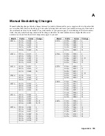
Page 166: ...Figure 6 9 Power Transformer Wiring Diagram for Models 655xA and 665xA Sheet 2 of 3 166 Diagrams ...

Page 167: ...Figure 6 9 Power Transformer Wiring Diagram for Models 655xA and 665xA Sheet 3 of 3 Diagrams 167 ...

Page 168: ......
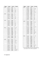
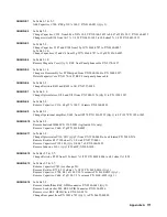
Page 169: ...3548A 00338 20 3619A 00393 24 6543A 3218A 00113 5 3425A 00218 17 3619A 00408 24 6544A 3219A 00113 5 3433A 00163 17 3620A 00233 24 6545A 3215A 00118 5 3408A 00148 15 3434A 00168 17 3623A 00218 24 6551A 3207A 00103 4 3424A 00153 17 3533A 00218 19 3549A 00223 20 21 3624A 00228 24 25 6552A 3203A 00103 4 3423A 00228 17 3526A 00323 19 3541A 00403 20 3548A 00503 21 3619A 00758 24 3632A 00798 25 Model Pre...

Page 170: ... 3519A 02031 19 3541A 02361 20 3548A 02641 21 22 3617A 02861 24 25 Model Prefix Serial Change 6653A 3006A 00121 7 3020A 00171 8 14 3035A 00331 3 9 3120A 00381 6 3128A 00659 11 3136A 00491 12 13 3216A 00661 5 3234A 00741 2 3347A 01091 16 3502A 01481 18 3548A 02121 21 3602A 02191 22 3619A 02361 24 3621A 02381 25 6654A 3007A 00121 7 3021A 00141 8 14 3035A 00241 9 3036A 00251 3 3051A 00271 6 3114A 003...

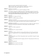
Page 171: ... 100 V Ceramic P N 0160 4803 CHANGE 9 In Table 5 5 Change Operational amplifier U605 from OP270 P N 1826 2252 Qty 1 to LT 1057 P N 1826 1845 CHANGE 10 In Table 5 5 Remove heatsink HS600 P N 1205 0282 Agilent 6651A only Remove Capacitor C646 47 pf P N 0160 4805 CHANGE 11 In Table 5 9 Change Optoisolator Ul10 Ul11 Qty 2 from P N 1990 0444 to Lead formed P N 5080 2176 Remove Resistor R137 100 ohm 1 1...

Page 172: ... to p n 5060 3315 NOTE Do not mix the 5060 3315 FET assemblies with the 5060 3314 FET assemblies in the SAME instrument CHANGE 20 In Tables 5 5 5 11 and 5 12 Change Q202 204 208 302 304 306 and 308 from p n 5060 3315 to p n 5060 3314 NOTE Do not mix the 5060 3315 FET assemblies with the 5060 3314 FET assemblies in the SAME instrument CHANGE 21 In Table 5 7 Change Y501 to 12 MHz p n 0410 2109 CHANG...

Page 173: ...59 83 86 CC load and line regulation 16 CC noise PARD 17 CC setup 15 CC source effect test 17 Circuits comparator 83 front panel board 89 isolator board 91 left tunnel 86 Output power control 86 87 right tunnel 86 Comparator circuits 83 Constant voltage tests CV setup 13 Conventions 200 W Vs 500 W 7 GPIB Vs Analog Programmable 7 Current monitoring resistor 11 Current programming and readback accur...

Page 174: ...90 EEPROM unique programmed data 90 Electronic load 11 Electrostatic discharge conductive table mat 8 Electrostatic discharge 8 Error output current measurement 11 F Firmware revisions front panel ROM chip 8 GPIB board ROM chip 8 IDN query 8 Form performance test record 19 Four terminal device 13 Functional circuit differences 83 G GPIB board circuits 90 GPIB controller primary address 90 secondar...

Page 175: ...panel 89 Loads electronic 11 M Manual revisions 8 Manuals operating 8 Measurement techniques 11 Model differences between Al main board heat sink assembly 86 N Negative logic signals asterisk vs bar 7 O Ordering parts 95 Overall troubleshooting procedures 34 37 40 P PARD CC constant current 17 PARD CC noise 17 PARD CV noise 14 PARD periodic and random deviations 17 PARD tests 11 Index 175 ...

Page 176: ...nel 13 from GPIB controller 13 remotely 13 R Recovery transient time 15 Regulation tests of DC current 16 Remote sensing leads 11 72 Replaceable parts 96 for 200 watt main chassis 96 Resistors current monitoring 11 fixed load 11 variable load 11 S Safety considerations hazardous voltages 8 safety symbols 3 SA secondary interface exiting test 46 48 SA signals A5 microprocessor 46 48 SA signals seco...

Page 177: ...rminal strip 91 Test equipment required 9 10 Test points 139 for Al main board 141 for A4A1 A4A3 left tunnel board 143 for A4A2 A4A4 right tunnel board 144 for GPIB board 140 for isolator board 140 Test procedures 11 Test record tables 11 Tests basic test set up 11 CC noise PARD 17 CC setup 15 CC source effect 17 current programming 15 current sink operation and readback 16 CV load effect 14 CV No...

Page 178: ...ccuracy 13 Tests power supply abnormal results 9 built in 9 performance 9 verification 9 Transformer AC input connections 137 Transient recovery time 15 Transient response waveform 15 V Verification operation tests 11 Verification tests 9 Voltage and current values 13 Voltage programming and readback accuracy 13 W Wait statements 11 Waveform transient response 15 178 Index ...

Page 179: ...ng updates have been made to this manual since its publication date 8 28 08 The performance test records on pages 20 29 have been updated to remove the measurement uncertainties and correct minor discrepancies in the test limits ...

Reviews: