90
C.9 Clear Interrupt and FIFO — BASE+8 and BASE+9
Writing data to either of these two bytes clears the interrupt or the
FIFO.
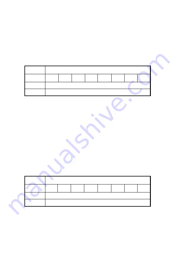
Table C-9: Register to clear interrupt and FIFO
Write
Clear Interrupt and FIFO
Bit #
7
6
5
4
3
2
1
0
BASE + 9
Clear FIFO
BASE + 8
Clear Interrupt
C.10 D/A Output Channel 0 — BASE+10 and BASE+11
The MIC-3716 provides an innovative design as
gate control
for the
Analog Output function. It works as a general Analog Output function
when you disable the flag (bit 3 (DA0_LDEN) of BASE+14). That
means data will be output immediately. However, when you enable the
flag, you need to read these two registers BASE+10 and BASE+11 to
output the data to the Analog Output channel.
Table C-10: Register for load D/A channel 0 data
Read
Load D/A Channel 0 data
Bit #
7
6
5
4
3
2
1
0
BASE + 11
BASE + 10
Summary of Contents for MIC-3716
Page 2: ...ii This page is left blank for hard printing...
Page 6: ...vi This page is left blank for hard printing...
Page 8: ...viii Table E 2 D A binary code table 117...
Page 11: ...1 Introduction 1 CHAPTER...
Page 17: ...7 Fig 1 1 Installation Flow Chart...
Page 21: ...11 Installation and Configuration CHAPTER 2...
Page 40: ...30 This page is left blank for hard printing...
Page 41: ...31 Signal Connections CHAPTER 3...
Page 44: ...34 Fig 3 1 I O connector pin assignments for the MIC 3716...
Page 50: ...40...
Page 54: ...44 This page is left blank for hard printing...
Page 55: ...45 Software Programming Overview CHAPTER 4...
Page 60: ...50 This page is left blank for hard printing...
Page 61: ...51 Calibration CHAPTER 5...
Page 77: ...67 Appendixes...
Page 81: ...71 Appendix B Block Diagrams...
Page 82: ...72 This page is left blank for hard printing...
Page 120: ...110 This page is left blank for hard printing...


