TF5/TF3/TF1
194
FADER CALIBRATION
Fader calibration should be done before starting the product test.
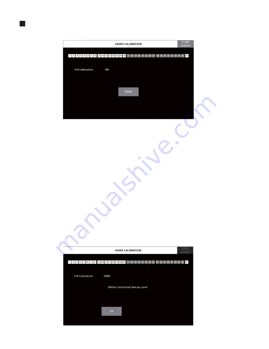
Startup the FADER CALIBRATION MODE screen and calibrate the faders according to directions of the screen.
1. Procedure
1) The button in an LCD screen
[START]
is touched. Since a con
fi
rmation screen is displayed, if
[OK]
is pushed, a calibration will
start.
2) All the faders chosen since it was displayed on the LCD screen as
"MOVE ALL SELECTED FADERS TO -∞dB and Press 'NEXT' Button"
are united with the index of -
∞
, and NEXT is performed.
3) All the faders chosen since it was displayed on the LCD screen as
"MOVE ALL SELECTED FADERS TO -20dB and Press 'NEXT' Button"
are united with the index of -20, and NEXT is performed.
4) All the faders chosen since it was displayed on the LCD screen as
"MOVE ALL SELECTED FADERS TO 0dB and Press 'NEXT' Button"
are united with the index of 0, and NEXT is performed.
5) All the faders chosen since it was displayed on the LCD screen as
"MOVE ALL SELECTED FADERS TO +10dB and Press 'NEXT'
Button"
are united with the index of +10, and NEXT is performed.
6) Since it is displayed on an LCD screen as
"[Motor Calibration] Are you sure ?"
and the calibration of a motor drive starts, don't touch
a fader until it ends.
There is no fader which carries out oscillation vibration about 1 second in each stop position, or it performs visual con
fi
rmation.
Содержание TF5
Страница 10: ...10 TF5 TF3 TF1 866 716 225 599 225 599 TF5 TF3 Unit mm Unit mm DIMENSIONS...
Страница 11: ...11 TF5 TF3 TF1 225 510 599 TF1 Unit mm...
Страница 110: ...B B MAIN MAINCOM Circuit Board 2NA0 ZJ06330 3 110 TF5 TF3 TF1...
Страница 111: ...B B Scale 90 100 Pattern side 2NA0 ZJ06330 3 111 TF5 TF3 TF1...
Страница 112: ...WR 3 1 1 WR 1 WR 0 1 1 WR 36 1 WR 1 DA1 DACOM Circuit Board Component side 2NA ZJ06450 1 112 TF5 TF3 TF1...
Страница 113: ...WR 1 WR 1 DA2 Circuit Board Scale 90 100 Component side 2NA ZJ06430 2 113 TF5 TF3 TF1...
Страница 116: ...WR 1 WR 1 7 WR 32 5 6 C C PS Circuit Board 2NA ZJ06320 2 116 TF5 TF3 TF1...
Страница 119: ...Component side D D Component side 2NA ZJ06380 4 119 TF5 TF3 TF1...
Страница 120: ...7 WR 31 1 7 WR 31 1 7 WR 31 1 WR 31 1 WR 31 1 QRW LQVWDOOHG E E PNC PNCOM Circuit Board 2NA ZJ06380 4 120 TF5 TF3 TF1...
Страница 166: ...TF5 TF3 TF1 166 q w e r PLAY q PASS FAIL w CLOSE USER DEFINED KEYS B...
Страница 201: ...TF5 TF3 TF1 201 USB 1 1GByte USB FAT32 2 1 YSISS TF updater v bin USB root 2 USB TF USB 3 4 LCD Update 5 LCD 6 LCD Close...
Страница 202: ...TF5 TF3 TF1 202 7 SYSTEM SETUP ABOUT 8 HOME Initialize All Memory CANCEL OK OK EXIT...


