TF5/TF3/TF1
148
HAAD22 AXR0[7](A6) of DSP#4(IC401) –>
OMNI1-8(11
th
) of CN705
SD_HA2(6
th
) of CN702 –>
AXR2[1](B7) of DSP#2(IC201)
HAAD31 AXR0[8](B6) of DSP#4(IC401) –>
OMNI9-16(13
th
) of CN705
SD_HA3(6
th
) of CN703 –>
AXR2[2](A7) of DSP#1(IC101)
HAAD32 AXR0[8](B6) of DSP#4(IC401) –>
OMNI9-16(13
th
) of CN705
SD_HA3(6
th
) of CN703 –>
AXR2[2](A7) of DSP#2(IC201)
HAAD41 AXR0[8](B6) of DSP#4(IC401) –>
OMNI9-16(13
th
) of CN705
SD_HA4(6
th
) of CN704 –>
AXR2[3](D8) of DSP#1(IC101)
HAAD42 AXR0[8](B6) of DSP#4(IC401) –>
OMNI9-16(13
th
) of CN705
SD_HA4(6
th
) of CN704 –>
AXR2[3](D8) of DSP#2(IC201)
AMUTE /MUTEOUT[4](72
nd
) of CPLD(IC802) –>
/A-MUTE(2
nd
) of CN705
7-7-2. ANA_UVLO
* Implemented in the MAINCOM circuit board test
[Contents]
Inspect the connection between the UVLO signal from PS
circuit board.
Connect the 10
th
pin of CN901 or TL901 to GND for a
moment and judge by detecting analog outputs are muted.
[Procedure]
<GUI>
Set [UVLO] to LOW level.
ABORT
Since popup dialog as shown in the above
fi
gure is displayed
on the screen, connect the 10
th
pin of CN901 or TL901 to
GND.
If operation is detected, popup dialog will be closed
automatically.
When popup dialog does not close in spite of having operated
it, it failed in the inspection.
Push the
[ABORT]
button to close the popup dialog.
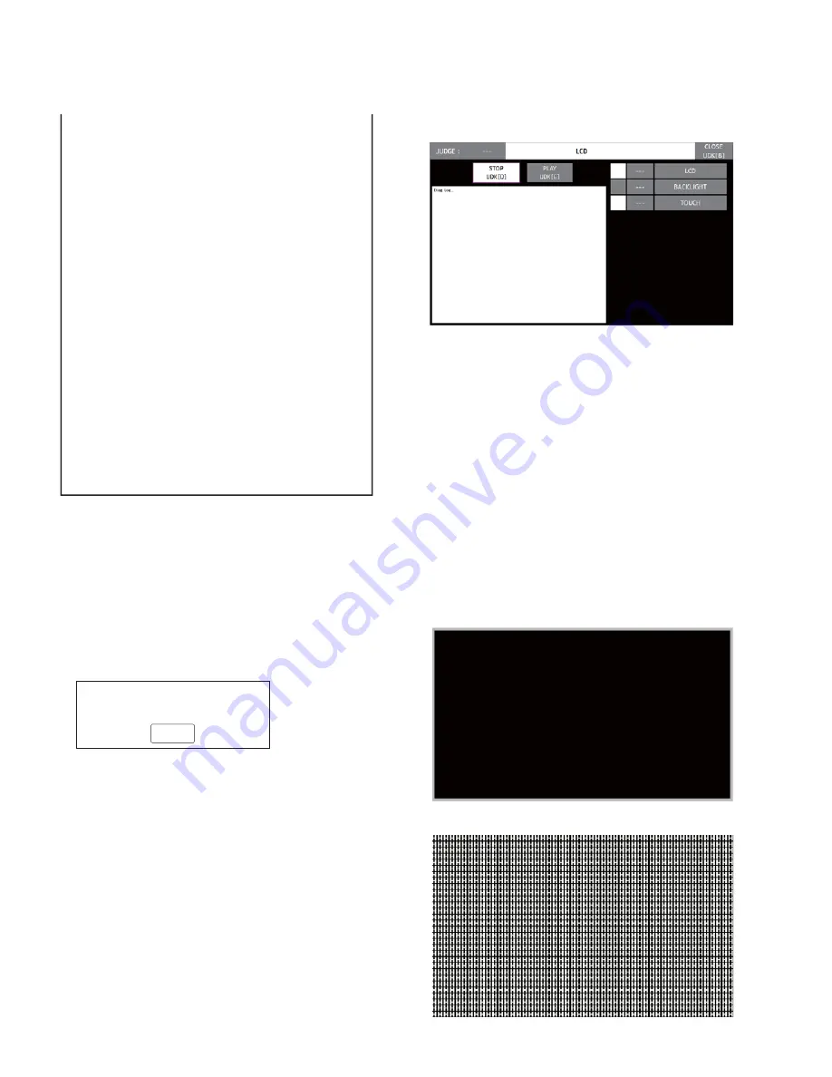
7-8. LCD
The example of a screen of the product test.
7-8-1. LCD
[Contents]
Inspect the LCD by checking the test pattern displayed on it.
[Procedure]
<GUI>
Check whether eight kinds of test patterns mentioned later
are displays as speci
fi
cation. If a
[TOUCH AND TURN]
knob is turned clockwise, the next screen will be displayed,
and it is displayed that the previous screen turns a
[TOUCH
AND TURN]
knob counterclockwise. Or if the right half of
an LCD screen is touched, it will go to the next screen, and if
a left half is touched, it can also return to a precious screen.
<TEST PATTERN>
1) Out frame 1dot
2) H character
Содержание TF5
Страница 10: ...10 TF5 TF3 TF1 866 716 225 599 225 599 TF5 TF3 Unit mm Unit mm DIMENSIONS...
Страница 11: ...11 TF5 TF3 TF1 225 510 599 TF1 Unit mm...
Страница 110: ...B B MAIN MAINCOM Circuit Board 2NA0 ZJ06330 3 110 TF5 TF3 TF1...
Страница 111: ...B B Scale 90 100 Pattern side 2NA0 ZJ06330 3 111 TF5 TF3 TF1...
Страница 112: ...WR 3 1 1 WR 1 WR 0 1 1 WR 36 1 WR 1 DA1 DACOM Circuit Board Component side 2NA ZJ06450 1 112 TF5 TF3 TF1...
Страница 113: ...WR 1 WR 1 DA2 Circuit Board Scale 90 100 Component side 2NA ZJ06430 2 113 TF5 TF3 TF1...
Страница 116: ...WR 1 WR 1 7 WR 32 5 6 C C PS Circuit Board 2NA ZJ06320 2 116 TF5 TF3 TF1...
Страница 119: ...Component side D D Component side 2NA ZJ06380 4 119 TF5 TF3 TF1...
Страница 120: ...7 WR 31 1 7 WR 31 1 7 WR 31 1 WR 31 1 WR 31 1 QRW LQVWDOOHG E E PNC PNCOM Circuit Board 2NA ZJ06380 4 120 TF5 TF3 TF1...
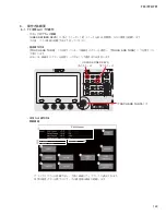
Страница 166: ...TF5 TF3 TF1 166 q w e r PLAY q PASS FAIL w CLOSE USER DEFINED KEYS B...
Страница 201: ...TF5 TF3 TF1 201 USB 1 1GByte USB FAT32 2 1 YSISS TF updater v bin USB root 2 USB TF USB 3 4 LCD Update 5 LCD 6 LCD Close...
Страница 202: ...TF5 TF3 TF1 202 7 SYSTEM SETUP ABOUT 8 HOME Initialize All Memory CANCEL OK OK EXIT...


