


ZC706 Evaluation Board User Guide
34
UG954 (v1.5) September 10, 2015
Feature Descriptions
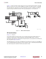
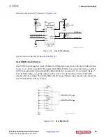
lists the pin-to-pin connections from each clock source to the XC7Z045 AP SoC.
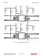
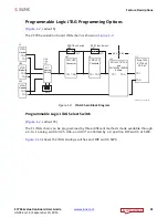
System Clock
[
, callout 7]
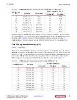
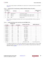
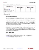
Table 1-12:
ZC706 Evaluation Board Clock Sources
Clock Name
Clock Source
Description
System Clock
U64
SiT9102 2.5V LVDS 200 MHz fixed-frequency oscillator (SiTime).
See
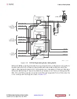
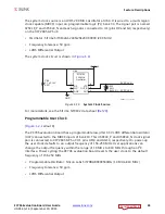
User Clock
U37
Si570 3.3V LVDS I
2
C programmable oscillator, 156.250 MHz default
(Silicon Labs). See
Programmable User Clock, page 35
.
User SMA Clock
J67(P), J68(N) User clock input SMAs, limit input swing voltage to VADJ_FPGA setting
(1.8V, 2.5V, 3.3V). See
User SMA Clock Source, page 36
PS Clock
U24
SIT8103 1.8V single-ended CMOS 33.3333 MHz fixed frequency
oscillator (SiTime). See
Processing System Clock Source, page 37
GTX SMA REF Clock
J36(P), J31(N) User clock input SMAs. See
GTX SMA Clock (SMA_MGT_REFCLK_P and
Jitter Attenuated Clock
U60
Si5324C LVDS precision clock multiplier/jitter attenuator (Silicon Labs).
See
Jitter Attenuated Clock, page 38
.
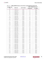
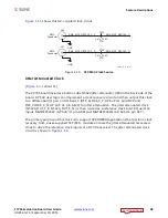
Table 1-13:
Clock Connections, Source to XC7Z045 AP SoC
Clock Source Pin
Net Name
I/O Standard
XC7Z045 (U1) Pin
U64.5
SYSCLK_N
LVDS
G9
U64.4
SYSCLK_P
LVDS
H9
U37.5
USRCLK_N
LVDS_25
AG14
U37.4
USRCLK_P
LVDS_25
AF14
J67.1
USER_SMA_CLOCK_P
LVDS_25
AD18
J68.1
USER_SMA_CLOCK_N
LVDS_25
AD19
J24.3
PS_CLK
NA(1)
A22 (Bank 500)
J36.1
SMA_MGT_REFCLK_P
NA(1)
W8
J31.1
SMA_MGT_REFCLK_N
NA(1)
W7
U60.29
SI5324_OUT_C_N
NA(1)
AC7
U60.28
SI5324_OUT_C_P
NA(1)
AC8
U60.17
REC_CLOCK_C_N
LVDS_25
AE20
U60.16
REC_CLOCK_C_P
LVDS_25
AD20
U60.3
SI5324_INT_ALM_LS
LVCMOS25
AJ25
U60.1
SI5324_RST_LS
LVCMOS25
W23
Notes:
1. PS-side and GTX nets do not have an assigned I/O standard.


