
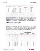

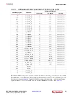


ZC706 Evaluation Board User Guide
35
UG954 (v1.5) September 10, 2015
Feature Descriptions
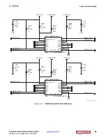
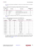
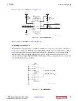
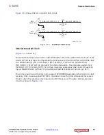
The system clock source is an LVDS 200 MHz oscillator at U64. It is wired to a multi-region
clock capable (MRCC) input on programmable logic (PL) bank 34. The signal pair is named
SYSCLK_P and SYSCLK_N and each signal is connected to U1 (pins H9 and G9, respectively)
on the XC7Z045 AP SoC.
• Oscillator: SiTime SiT9102AI-243N25E200.00000 (200 MHz)
• Frequency tolerance: 50 ppm
• LVDS Differential Output
The system clock circuit is shown in
For more details, see the SiTime SiT9102 data sheet
.
Programmable User Clock
[
, callout 8]
The ZC706 evaluation board has a programmable low-jitter 3.3V LVDS differential oscillator
(U37) connected to the MRCC inputs of bank 10. This USRCLK_P and USRCLK_N clock signal
pair is connected to XC7Z045 AP SoC U1 pins AF14 and AG14, respectively. On power-up
the user clock defaults to an output frequency of 156.250 MHz. User applications can
change the output frequency within the range of 10 MHz to 810 MHz through an I
2
C
interface. Power cycling the ZC706 evaluation board reverts the user clock to the default
frequency of 156.250 MHz.
• Programmable Oscillator: Silicon Labs Si570BAB0000544DG (10 MHz–810 MHz)
• Frequency tolerance: 50 ppm
• LVDS Differential Output
X-Ref Target - Figure 1-11
Figure 1-11:
System Clock Source
UG954_c1_11_041113
GND
VCC2V5
SIT9102
200 MHz
Oscillator
OE
NC
GND
VCC
OUT_B
OUT
1
2
3
6
5
4
U64
R322
100
Ω
1/20W 5%
SYSCLK_P
SYSCLK_N
C89
0.1
µ
F 10V
X5R
1
2
2
1


