


ZC706 Evaluation Board User Guide
38
UG954 (v1.5) September 10, 2015
Feature Descriptions
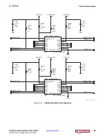
shows this AC-coupled clock circuit.
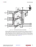
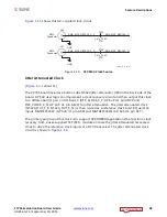
Jitter Attenuated Clock
[
, callout 11]
The ZC706 board includes a Silicon Labs Si5324 jitter attenuator U60 on the back side of the
board. AP SoC user logic can implement a clock recovery circuit and then output this clock
to a differential I/O pair on I/O bank 9 (REC_CLOCK_C_P, AP SoC U1 pin AD20 and
REC_CLOCK_C_N, AP SoC U1 pin AE20) for jitter attenuation. The jitter attenuated clock
(Si5324_OUT_C_P, Si5324_OUT_C_N) is then routed as a reference clock to GTX Quad 110
inputs MGTREFCLK1P (AP SoC U1 pin AC8) and MGTREFCLK1N (AP SoC U1 pin AC7).
The primary purpose of this clock is to support CPRI/OBSAI applications that perform clock
recovery from a user-supplied SFP/SFP+ module and use the jitter attenuated recovered
clock to drive the reference clock inputs of a GTX transceiver. The jitter attenuated clock
circuit is shown in
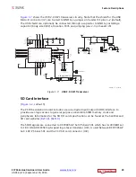
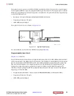
X-Ref Target - Figure 1-15
Figure 1-15:
GTX SMA Clock Source
UG954_c1_15_041113
SMA_MGT_REFCLK_P
SMA_MGT_REFCLK_C_P
SMA
Connector
J36
GND
C145
0.01
μ
F 25V
X7R
SMA_MGT_REFCLK_N
SMA_MGT_REFCLK_C_N
SMA
Connector
J31
GND
C144
0.01
μ
F 25V
X7R


