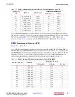

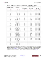


ZC706 Evaluation Board User Guide
36
UG954 (v1.5) September 10, 2015
Feature Descriptions
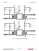
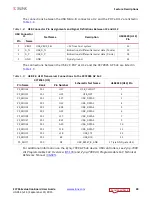
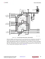
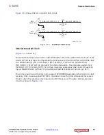
The user clock circuit is shown in
.
See the Silicon Labs Si570 data sheet
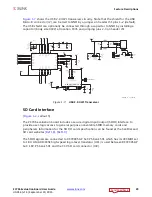
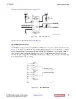
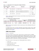
User SMA Clock Source
The ZC706 board provides a pair of SMAs for differential user clock input into PL Bank 9 (see
). The P-side SMA J67 signal USER_SMA_CLOCK_P is connected to U1 pin AD18,
with the N-side SMA J68 signal USER_SMA_CLOCK_N connected to U1 pin AD19. Bank 9
Vcco is VADJ_FPGA, a variable voltage (1.8V, 2.5V, 3.3V) depending on the ZC706 FMC
interface banks voltage. The USER_SMA_CLOCK input voltage swing should not exceed the
board VADJ_FPGA voltage setting.
X-Ref Target - Figure 1-12
Figure 1-12:
User Clock Source
X-Ref Target - Figure 1-13
Figure 1-13:
User SMA Clock
UG954_c1_12_041113
GND
VCC3V3
1
2
3
8
7
6
U37
R37
4.7K
Ω
1/10W
5%
C348
0.01
μ
F 25V
X7R
4
5
GND
VCC3V3
10 MHz-810 MHz
50PPM
Si570
Programmable
Oscillator
NC
OE
GND
SCL
SDA
VDD
OUT_B-
OUT+
R323
100
Ω
1/20W 5%
USRCLK SFP SDA
USRCLK SFP SCL
USRCLK N
USRCLK P
1
2
1
2
1
2
UG954_c1_13_041113


