
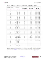


ZC706 Evaluation Board User Guide
37
UG954 (v1.5) September 10, 2015
Feature Descriptions
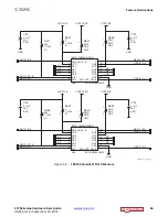
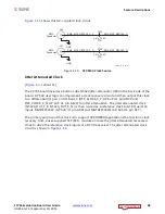
Processing System Clock Source
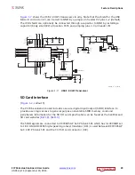
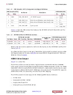
The Processing System (PS) clock source is a 1.8V LVCMOS single-ended fixed
33.33333 MHz oscillator at U24. It is wired to PS bank 500, pin A22 (PS_CLK), on the
XC7Z045 AP SoC.
• Oscillator: SiTime SiT8103AC-23-18E-33.33333 (33.3 MHz)
• Frequency tolerance: 50 ppm
• Single-ended output
The system clock circuit is shown in
For more details, see the SiTime SiT8103 data sheet
.
GTX SMA Clock (SMA_MGT_REFCLK_P and SMA_MGT_REFCLK_N)
[
, callout 10]
The ZC706 board includes a pair of SMA connectors for a GTX clock wired to GTX Quad bank
111. This differential clock has signal names SMA_MGT_REFCLK_P and SMA_REFCLK_N,
which are connected to AP SoC U1 pins W8 and W7 respectively.
• External user-provided GTX reference clock on SMA input connectors
• Differential Input
X-Ref Target - Figure 1-14
Figure 1-14:
Processing System Clock Source
UG954_c1_14_041113
GND
VCCP1V8
SiT8103
Oscillator
33.33333 MHz
50 PPM
OE
GND
VCC
1
2
4
U24
R38
4.7K
Ω
1/10W
5%
C349
0.01
μ
F 25V
X7R
3
GND
VCCP1V8
OUT
R173
24.9
Ω
1/10W 1%
PS CLK
1
2
1
2
1
2


