background image

DNA/DNR-429-512/566 ARINC 429 Layer


Chapter 1

4

Introduction

Tel:  508-921-4600

www.ueidaq.com

Vers: 

4.5


Date: December 2013 

 DNx-429-Chap1x.fm

© Copyright 2013


United Electronic Industries, Inc.

1.3

Features

The common features of the DNx-429-512/566 are listed below:

12 ARINC 429 channels configured as 6TX/6RX channels 


(DNA-429-566) or 12 RX channels (DNA-429-512)

High Current (350 mA max), Low-Side FET General Purpose Digital 
Output with 500 mA resettable fuse

High Speed (100 kHz) or Low Speed (12.5 kHz), selectable per port pair

Hardware Label filtering

Hardware Transmit Scheduler (100 uS timing resolution)

Automatic timestamping of data, software enabled/disabled

Tested to withstand 5g Vibration, 50g Shock, -40 to +85°C Temperature, 
and Altitude up to 70,000 ft or 21’000 meters.

Weight of 104 g or 3.7 oz for DNA-429-512/566; 4.1 oz for DNR-429.

UEI Framework Software API may be used with all popular Windows 
programming languages and most real time operating systems such as 
RT Linux, RTX, or QNX and graphical applications such as LabVIEW, 
MATLAB, DASYLab and any application supporting ActiveX or OPC.


1.4

Indicators

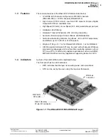
A photo of the 429-512/566 unit is illustrated below.
The front panel has two LED indicators:

RDY: indicates that the layer is receiving power and operational.

STS: can be set by the user using the low-level framework. 


DB-37 (female) 
37-pin I/O connector 

RDY LED
 STS LED

DNA bus
connector

Figure 1-1.  The DNA-429-512/566 ARINC-429 Layer


Содержание DNA 429-512

Страница 1: ...12 Channel ARINC 429 Transmitter Receiver Interface Layer for the PowerDNA Cube and PowerDNR RACKtangle Release 4 5 December 2013 PN Man DNx 429 512 566 1213 Copyright 1998 2013 United Electronic Industries Inc All rights reserved ...

Страница 2: ... 2350 Also see the FAQs and online Live Help feature on our web site Internet Support Support support ueidaq com Web Site www ueidaq com FTP Site ftp ftp ueidaq com Product Disclaimer WARNING DO NOT USE PRODUCTS SOLD BY UNITED ELECTRONIC INDUSTRIES INC AS CRITICAL COMPONENTS IN LIFE SUPPORT DEVICES OR SYSTEMS Products sold by United Electronic Industries Inc are not authorized for use as critical ...

Страница 3: ...5 Specification 5 1 6 Device Architecture 6 1 6 1 Word Format 8 1 6 2 Receiver Block 10 1 7 3 Label Acceptance Filter 12 1 8 4 Transmitter Block 13 1 8 5 Scheduler 14 1 9 Wiring Connectors 17 Chapter 2 Programming with the High Level API 18 2 1 Creating a Session 18 2 2 Configuring the Resource String 18 2 3 Configuring the Timing 19 2 4 Read Data 20 2 5 Write Data 20 2 6 Programming the Output Sc...

Страница 4: ...ries Inc List of Figures 1 1 Typical Schematic Diagram for FET Digital Output DOUT0 3 1 2 The DNA 429 512 566 ARINC 429 Layer 4 1 3 DNA DNR 429 512 566 Logic Block Diagram 6 1 4 ARINC 429 Waveform Characteristics 7 1 5 General ARINC Word Format 8 1 6 Receiver Diagram 11 1 7 Transmitter Block Diagram Hardware Abstraction Layer 13 1 8 DNx 429 512 566 Pinout Diagram 17 ...

Страница 5: ...on provides an overview of the 429 512 566 ARINC interface board features device architecture and connectivity Programming with the High Level API This chapter provides an overview of the how to create a session configure the session and format relevant data with the Framework API Programming with the Low Level API Describes low level API commands for configuring and using the 429 512 566 series l...

Страница 6: ...ce generally represents text that should be entered verbatim For instance it can represent a command as in the following example You can instruct users how to run setup using a command such as setup exe Text formatted in fixed typeface generally represents source code or other text that should be entered verbadim into the source code initialization or other file Examples of Manual Conventions Befo...

Страница 7: ...ure data integrity 256 word FIFOs are provided on every TX and RX channel In addition the DNx 429 566 512 ARINC layer has 3x current sinking 350 mA max low side FET general purpose digital output with 500 mA resettable fuse Software supplied with the boards permits you to select options such as Receive Filter size 1 to 255 or disable Source Destination filter SDI enable disable Forward changed dat...

Страница 8: ...mping of data software enabled disabled Tested to withstand 5g Vibration 50g Shock 40 to 85 C Temperature and Altitude up to 70 000 ft or 21 000 meters Weight of 104 g or 3 7 oz for DNA 429 512 566 4 1 oz for DNR 429 UEI Framework Software API may be used with all popular Windows programming languages and most real time operating systems such as RT Linux RTX or QNX and graphical applications such ...

Страница 9: ...ons BUB SBUF L PS L 0 TJ F XPSET Transmit modes 4DIFEVMFE PS BTZODISPOPVT Scheduler specifications UJNJOH SFTPMVUJPO NJDSPTFDPOET UBCMF TJ F 4DIFEVMF VQ UP MBCFMT QFS DIBOOFM Asynchronous TX modes JHI QSJPSJUZ USBOTNJU JNNFEJBUFMZ VQPO DPNQMFUJPO PG DVSSFOU USBOTNJTTJPO SFHBSEMFTT PG TDIFEVMF 4UBOEBSE QSJPSJUZ transmit when no scheduled data 0 CBTFE USBOTNJU XIFO OP TDIFEVMFE TUBOEBSE PS IJHI QSJPS...

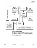
Страница 10: ...elector error reporting etc TX Port Access Controller RX0 channel FPGA DSP block 2RX 1TX ARINC 429 transceiver protocol controllers FPGA DSP control access Block 0 SDI Filter Label Acceptance Filter RX FIFO with Timestamp ARINC 429 RX TX Block 1 ARINC 429 RX TX Block 2 ARINC 429 RX TX Block 3 ARINC 429 RX TX Block 4 ARINC 429 RX TX Block 5 RX6 channel FPGA DSP block data data data control control ...

Страница 11: ... on a per channel or port pair basis see page 10 The transmission medium for an ARINC 429 bus is 78 ohm twisted shielded pair cable grounded at both ends and at any break in the cable shield Each bus has only one transmitter and up to 20 receivers Since data transmission is uni directional only transmitters and receivers are on separate ports The waveform characteristics must conform to the specif...

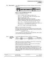
Страница 12: ...in which bits are transmitted received is somewhat complex the HI 3282 chips handle the decoding automatically The bits are transmitted on the ARINC bus in the following order 8 7 6 5 4 3 2 1 9 10 11 12 32 The Label first 8 bits is transmitted before the data MSB first After the label is sent the LSB of each byte is transmitted first 1 6 1 1 Scheduler ARINC Data Format The Scheduler ARINC Data For...

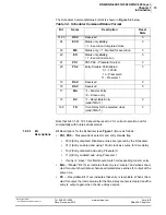
Страница 13: ...the AR566_ARDA0 register 10 9 10 9 31 30 SSM Sign Status matrix or data bits See ARINC 429 protocol documentation for details 8 8 32 PARITY Parity bit auto inserted by the transmitter and calculated by the receiver Normal parity for the ARINC 429 is odd Parity bit should be set if the number of 1 s in the rest of the bits is even and should be cleared if not DNA 429 layers support even odd or no p...

Страница 14: ...ou need to re calculate parity for bits 1 31 to deduce the actual value of the transmitted parity bit 1 6 2 Receiver Block As indicated in Figure 1 2 on page 6 the RX0 receiver in each Building Block has a software selectable label acceptance filter that accepts or rejects incoming data words As an option you can choose to accept only changed data This option uses the last received data memory and...

Страница 15: ... ARINC 429 Receiver ARINC 429 Receiver Hardware Raw Frame 255 entry Label Acceptance Filter Timestamp Source Parity Error Bit Checker Data Change Checker RX FIFO Trigger Generator Last Data Memory RX Frame Counter 32 bit 0x0 in the first entry disables bypasses filter entries skips them in the verification acceptance process for the Scheduler Available only for the RX0 receivers 256 x 32 256 x 32 ...

Страница 16: ...Only flag In new data only mode set via RX0 Control Register AR566_Rx and if this bit is set only data that has changed since last reception is placed into the FIFO and the last data memory NOTE For the 566 model the new data only mode is not available on loopback receivers 0 7 LABEL Acceptance label If the label matches bits 7 0 of the received frame the frame is accepted by the filter NOTE 1 0x0...

Страница 17: ...transfer transmitter with a high and a low priority register The Scheduler transfers its data to the ARINC bus at a specified time interval either one time or continuously at user specified intervals Scheduled data may also be transferred in blocks based on a master slave entry scheme Also the Scheduler may be configured to transfer data when a predefined label with index is received from the labe...

Страница 18: ...ts data based on the priority scheme above and sends confirmation after the data is accepted for transmission NOTE The Scheduler and FIFO priorities may be interchanged by setting the FIFOHP bit in the AR566_ACCR register 1 8 5 Scheduler The Scheduler is programmed using two arrays in the memory address space dedicated to the Scheduler command and associated ARINC data Because of space limitations...

Страница 19: ...is slave this field should match corresponding master entry MA Master Bit If set indicates that entry is a master and when sched uled for output should also schedule all related slave entries for output at the same time RC Recyclable Bit If set indicates that entry is recyclable When sched uled for output the internal value for the time delay counter is cleared and the entry is output again when t...

Страница 20: ...ns of the Status only bits are as follows ECO Execution Complete at Least Once If set this bit indicates that the entry was output by the ARINC transmitter at least once This is a sticky bit that can be cleared only by writing a command to the Scheduler This com mand may change or may stay the same NOTE Writing to the Scheduler command area clears some internal status bits It is recommended that y...

Страница 21: ... 0 to TX B 5 and the six RX channels are numbered as RX A 0 to RX A 5 and RX B 0 to RX B 5 In the DNx 429 512 the 12 RX lines are numbered as RX A 0 to RX A 11 and RX B 0 to RX B 11 Each general purpose digital output line has a current sinking 350mA max low side FET with 100kΩ pull up for 5V Output pin may be left floating or grounded Each line is protected by a 500 mA resettable fuse between FET...

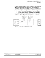
Страница 22: ...nd all other devices are slaves receiving only The physical medium between master and slave s is two twisted pair wires carrying a differential signal a is for the non inverting signal may be inaccurately labelled as b is for the inverting signal may also be inaccurately labelled as The signals from a b lines are with reference to the ground Even though the configuration in Figure 1 8 is common ot...

Страница 23: ...ring UeiDaq Framework uses resource strings to select which device subsystem and channels to use within a session The resource string syntax is similar to a web URL device class IP address Device Id Subsystem Channel list For PowerDNA and RACKtangle the device class is pdna ARINC layers have dedicated input and output ports Use the ATX token for the output subsystem and the ARX token for the input...

Страница 24: ...t receives less than 10 words per second it will return whatever number of words is available every second Configure ARINC output ports 0 2 5 on device 0 session CreateARINCOutputPort pdna 192 168 100 2 Dev0 ATX0 2 5 UeiARINCBitsPerSecond12500 UeiARINCParityOdd typedef struct _tUeiARINCWord The label of the word It is used to determine the data type of the Data field and therefore the method of da...

Страница 25: ...ect per output port to be able to write to each port in the port list The following sample code shows how to create a writer object tied to Port 2 and send one word to the ARINC bus 2 6 Programming the Output Scheduler Each output channel is equipped with a hardware Scheduler that you can use to send sequences of ARINC words at a given rate without intervention of the host or and or software Creat...

Страница 26: ...encies you must first stop the session and then add additional words in the existing sequence or clear the Scheduler with the following call Configure ARINC output ports 0 2 5 on device 0 CUeiARINCOutputPort pPort dynamic_cast CUeiARINCOutputPort session GetChanel index typedef struct _tUeiARINCSchedulerEntry Specifies whether this is a master or slave entry Int32 Master Specifies whether this ent...

Страница 27: ...irst You can then add addi tional filters or clear the existing filters with the following call 2 8 Cleaning up the Session session CleanUp The session object will clean itself up when it goes out of scope or when it is destroyed To reuse the object with a different set of channels or parameters you can manually clean up the session as follows Get pointer to the input channel CUeiARINCInputPort pP...

Страница 28: ...vidual fields DqAdv566BuildFilterEntry Assembles filter entries from the separate fields DqAdv566BuildSchedEntry Assembles a scheduler entry from the separate fields DqAdv566SetConfig Configures basic ARINC device parameters DqAdv566SetMode Configures the mode of operation for each channel DqAdv566SetFilter This function writes to or reads from the label filter DqAdv566SetScheduler This function w...

Страница 29: ...A STP 37 provides easy screw terminal connections for all DNA and DNR series I O boards which utilize the 37 pin connector scheme The DNA STP 37 is connected to the I O board via either DNA CBL 37 or DNA CBL 37S series cables The dimensions of the STP 37 board are 4 2w x 2 8d x1 0h inch or 10 6 x 7 1 x 7 6 cm with standoffs The weight of the STP 37 board is 2 4 ounces or 69 grams DNA STP 37D The D...

Страница 30: ...entions 2 Creating a Session 18 D DNx 429 512 3 DNx 429 566 3 E Emergency Transfer Transmitter 14 F FIFO 13 H Hardware Abstraction Layer 13 High Level API 18 J Jumper Settings 17 L Label Acceptance Filter 12 Loopback Connection 10 Low level API 23 O Organization 1 P Prescalers 13 Priority Registers 13 R Receiver Block 10 Receiver Diagram 11 S Scheduler 13 14 Scheduler ARINC Data Format 8 Scheduler...

Отзывы: