DNA/DNR-429-512/566 ARINC 429 Layer
Chapter 1
17
Introduction
Tel: 508-921-4600
www.ueidaq.com
Vers:
4.5
Date: December 2013
DNx-429-Chap1x.fm
© Copyright 2013
United Electronic Industries, Inc.
1.9
Wiring &
Connectors
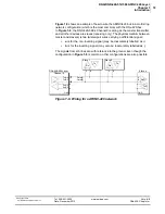
The following signals are located at the DB-37 female connector on the 429-512/
566 layer:
•
Rx-A-
n
: Receive line on bus A of channel
n
•
Rx-B-
n
: Receive line on bus B of channel
n
•
Tx-A/B-
n
: Transmit line on bus A (or B) on the 429-566
•
Trig-In: Trigger input
•
Dout
n
: Digital output line
The pinout for the 429-512/566 is provided below:
Figure 1-7. DNx-429-512/566 Pinout Diagram
Note
that in the DNx-429-566, the six TX channels are numbered as
TX-A-0 to TX-A-5 (and TX-B-0 to TX-B-5); and the six RX channels are
numbered as RX-A-0 to RX-A-5 (and RX-B-0 to RX-B-5).
In the DNx-429-512, the 12 RX lines are numbered as RX-A-0 to RX-A-11 (and
RX-B-0 to RX-B-11).
Each general purpose digital output line has a current sinking (350mA max) low-
side FET with 100k
Ω
pull-up for +5V. Output pin may be left floating or grounded.
Each line is protected by a 500 mA resettable fuse between FET and output pin.
Before plugging any I/O connector into the Cube or Layer, be sure
to remove power from all field wiring. Failure to do so may cause
severe damage to the equipment.
59"
39"
59"
39"
(OE
59"
39"
59"
$ML0VU
39"
59"
39"
59"
(OE
39"
3TWE0VU
%PVU
7ED
OD
59#
39#
59#
39#
5SJH*O
59#
39#
59#
(OE
39#
59#
39#
59#
3TWE*O
39#
%PVU
%PVU
(OE
39"
39"
39"
39"
(OE
39"
39"
39"
$ML0VU
39"
39"
39"
39"
(OE
39"
3TWE0VU
%PVU
7ED
OD
39#
39#
39#
39#
5SJH*O
39#
39#
39#
(OE
39#
39#
39#
39#
3TWE*O
39#
%PVU
%PVU
(OE
DNA-429-566
DNA-429-512


