background image


EVK-IRIS-W10 - User guide 

UBX-23007837 - R03 

Setting up the evaluation board  

Page 8 of 43 

C1-Public  


8.


Replace the 

flash_config.c

” in the 

SDK\boards\rdrw612bga\flash_config


folder 

with the 

updated version, which includes an updated FCB (Flash configuration block) and supports 
low-density Macronix 8MB QSPI Flash. The updated 

flash_config.c

 file is available in the 

u-blox short range open CPU GitHub repository

 [6].


2.1.2


Wi-Fi example application 

The wifi_cli application is provided in binary format and can be used to quickly demonstrated 
Wi-Fi features without the need of installing SDK or compiling any firmware. 

Example of supported features: 


Wi-Fi Scan 

o


Wi-Fi Soft AP mode 

o


Wi-Fi Station mode 


Throughput performance using 

iPerf 

measurement tool 

2.1.2.1


Flash the wifi_cli example firmware 

IRIS-W10 module stores the RW612 application and Wi-Fi firmware binary in different 
partitions of internal FlexSPI NOR flash. The application reads Wi-Fi firmware during 
initialization and downloads it to RW612 internal Wi-Fi MCU to run. 

1.


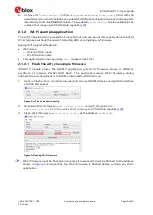
Open J-Flash Lite or JLinkCommander and connect RW612 device using SWD interface 
at 4000 kHz speed. 


Figure 2: J-Flash Lite device config 

2.


Download Wi-Fi firmware 

rw610_sb_wifi_v1.bin 

and


wifi_cli

 application


rw612_wifi_cli.hex


from the u-blox short range open CPU

 GitHub repositor

[6].


3.


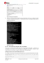
Flash Wi-Fi firmware 

rw610_sb_wifi_v1.bin


at the address


0x08400000


Figure 3: Flashing Wi-Fi firmware 


Wi-Fi firmware must be flashed once unless it is erased. It must be flashed to the address 
shown  in 

Figure 3

Ensure that the Wi-Fi firmware is flashed before running any Wi-Fi 

application. 

Содержание IRIS-W10 Series

Страница 1: ...es modules User guide Abstract This document describes how to set up and use the EVK IRIS W10 evaluation kits for prototyping the IRIS W10 open CPU multiradio modules It also describes the different o...

Страница 2: ...gos and designs included in this document Copying reproduction or modification of this document or any part thereof is only permitted with the express written permission of u blox Disclosure to third...

Страница 3: ...elopment 10 2 2 1 NXP SDK 10 3 Hardware description 11 3 1 Power 11 3 1 1 Powering the board 12 3 1 2 IRIS W10 module power 14 3 1 3 Current measurement 15 3 2 Reset 15 3 2 1 Automatic bootloader Boot...

Страница 4: ...EVK IRIS W10 User guide UBX 23007837 R03 Contents Page 4 of 43 C1 Public 3 13Jumpers 37 3 14Test points 40 Appendix 41 A Glossary 41 Related documentation 42 Revision history 43 Contact 43...

Страница 5: ...boards are designed to accommodate a diverse range of electronic modules including sensors transceivers displays encoders motor drivers connection ports and more For further information about the Clic...

Страница 6: ...4 supporting Thread Matter over Wi Fi and Ethernet Bluetooth LE subsystem supporting Bluetooth 5 3 in 2 4 GHz band Bluetooth LE central peripheral GATT client server roles LE Audio Peripherals1 ADC G...

Страница 7: ...or custom application development Before compiling custom software you must configure the NXP MCUXpresso SDK for use with the IRIS W10 open CPU variant For information about for the working environmen...

Страница 8: ...t performance using iPerf measurement tool 2 1 2 1 Flash the wifi_cli example firmware IRIS W10 module stores the RW612 application and Wi Fi firmware binary in different partitions of internal FlexSP...

Страница 9: ...Figure 5 wifi_cli demo 2 1 2 2 Run iperf test using the wifi_cli example This section assumes that the iperf test is run using two EVK IRIS W10 with Device A configured as an Access Point and Device...

Страница 10: ...a terminal session and enter wlan add test1 ssid NXPAP ip 192 168 10 3 192 168 10 1 255 255 255 0 channel 48 wpa2 12345678 wlan connect test1 iperf c 192 168 10 1 2 2 Software Development 2 2 1 NXP S...

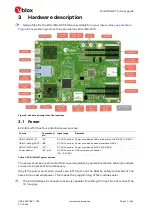
Страница 11: ...e IRIS W10 USB 1 USB C debug UART J98 5 0 VDC nominal Power provided by debug interface USB 2 USB C MCU LINK J101 5 0 VDC nominal Power provided by MCU LINK USB 3 Power header J42 pin 1 5 0 VDC nomina...

Страница 12: ...ections on pin headers mikroBUS slots 5 V positions There are two options for the maximum current for the EVK either Populate the 2 4 A power switch U6 MP5075GTF and disconnect R124 as shown in Figure...

Страница 13: ...ork with variable output voltage LDOs R288 and R211 provide an option to supply the MCU LINK chip from U11 output voltage 3 1 1 3 USB 2 0 On The Go OTG The OTG function is only supported on the module...

Страница 14: ...tion Otherwise they can only supply a combined 500mA current and should not be utilized in conjunction with USB OTG Host mode 3 1 1 5 mikroBUS slots 5 V positions Intended for mikroBUS standard 5 V pi...

Страница 15: ...ltage drop across pins 2 and 3 If the current sensor is removed from the circuit current can also be measured directly by opening J97 or J96 Use an ammeter in series with the two voltage pins If VDD I...

Страница 16: ...1 and CON0 respectively in the table shown in Figure 16 o For example to select ISP as boot source GND the signal EXT REQ on SW3 Alternatively other configurations are possible as described in the tab...

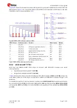
Страница 17: ...ootloader Bootstrap RESET SW5 PDn Resets the module FTDI chip and mikroBUS slots Table 3 User button definitions 3 4 User LEDs EVK IRIS W10 supports 16 LEDs Power status D10 Indicates 3V3 on the board...

Страница 18: ...3 CTS UART3 CTS activity indicator D8 Green GPIO11 UART3 DTR UART3 DTR activity indicator D9 Green GPIO12 UART3 DSR UART3 DSR activity indicator Table 5 UART3 LEDs and associated signals B 3 4 G 2 R 1...

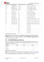
Страница 19: ...odule and a host computer MCU Link is based on the LPC55S69 microcontroller U13 and features a high speed USB interface for a high performance debugging The main UART UART 3 TX RX and the SWD interfac...

Страница 20: ...fault 86 GPIO 17 FC2 I2C_SCL Not default 76 GPIO 24 UART3 RXD Default 79 GPIO 26 UART3 TXD Default 70 Table 6 MCU Link connections The SWD programming interface on the MCU Link connects to the JTAG ne...

Страница 21: ...s valid when low Low R192 5 HW_VER_5 Power measurement enabled when low Low R193 56 HW_VER_6 VCOM disabled when low Float R194 27 HW_VER_7 SWD debug disabled when low Float R195 Table 7 MCU LINK hardw...

Страница 22: ...U109 A11 GPIO 11 UART DTR R56 FTDI UART DTR Pin 43 U108 Pin 18 U109 B10 GPIO 12 UART DSR R57 FTDI UART DSR Pin 44 U108 Pin 4 U109 R58 Pin 48 U108 R59 Pin 52 U108 R60 Pin 53 U108 R61 Pin 54 U108 R63 P...

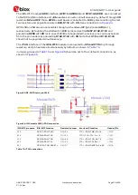
Страница 23: ...s can be accessed from the pin headers by populating R142 R143 with 0R Note that U19 and R142 R143 should not be populated simultaneously The JTAG interface of the IRIS W10 module is connected to J20...

Страница 24: ...enabled by default GPIO21 and GPIO23 multiplex some of the RMII signals and the external crystal oscillator option Figure 27 shows how to demultiplex those GPIOs To enable low frequency clock populat...

Страница 25: ...hare GPIO 27 as the PWM pin so this GPIO can only be used in a single slot GPIO 27 is enabled on slot 2 by default as shown in Table 12 and Table 13 All four mikroBUS slots share GPIO 18 as INT pin so...

Страница 26: ...1 mikroBUS 2 R11 R21 mikroBUS 3 R46 R70 mikroBUS 4 R10 R19 Table 14 mikroBUS RESET configuration resistors default connection 3 8 1 mikroBUS 1 slot This slot is connected to the Flexcomm interface 0 c...

Страница 27: ...ares GPIO 15 and GPIO 16 or as UART with SWD interface enabled U19 default connection disconnect R257 and populate R258 with 0R as shown in Figure 30 To enable this slot In case of USB switch U19 is p...

Страница 28: ...roBUS 3 slot This slot is connected to the Flexcomm interface 1 that cannot be used with the JTAG interface that shares all GPIOs on this slot as shown in Figure 32 To enable this slot Invert the defa...

Страница 29: ...erface 1 that cannot be used totally with RMII function which shares GPIO55 GPIO 56 and GPIO 57 as shown in Figure 33 To enable this slot Disconnect R111 R263 R265 and populate R115 R264 R266 with 0R...

Страница 30: ...demultiplex the RMII signals described in Table 19 from other functions that cannot be used simultaneously with RMII as shown in Figure 34 Group 1 Flexcomm F14 RX TX RTS signals populate R111 R263 R2...

Страница 31: ...GPIO23 RMII RXD1 R268 R139 PHY RXD1 Pin 15 J1 GPIO22 RMII RXD0 R272 PHY RXD0 Pin 16 L4 GPIO55 RMII INT R111 R149 PHY INT Pin 21 F3 GPIO25 RMII RXCLK R279 PHY RXCLK Pin 9 M2 GPIO21 RMII RESET R210 PHY...

Страница 32: ...iation Pull up default Enable Pull down Disable B_CAST_OFF Broadcast Off for PHY Address 0 Pull up PHY Address 0 set as unique PHY address Pull down default PHY Address 0 set as broadcast PHY address...

Страница 33: ...EVK IRIS W10 User guide UBX 23007837 R03 Hardware description Page 33 of 43 C1 Public Figure 36 SDIO schematic Figure 37 SDIO jumpers schematic...

Страница 34: ...GPIO15 SDIO CLK R100 J55 SDIO CLK A7 GPIO16 SDIO D3 R97 J56 SDIO D3 B7 GPIO17 SDIO CMD R98 J57 SDIO CMD B8 GPIO19 SDIO D0 R101 J58 SDIO D0 A9 GPIO20 SDIO D1 R102 J59 SDIO D1 B6 GPIO18 SDIO D2 R83 J60...

Страница 35: ...and U3 GPIO12 J10 7 Default and can t disconnect Disconnect R256 and U3 GPIO13 J47 2 Not default Disconnect R257 and populate U19 and R258 with 10K Or populate R143 with 0R GPIO14 J48 1 Not default Di...

Страница 36: ...and populate R278 with 0R GPIO60 J44 6 Not default Disconnect R280 and populate R283 with 0R GPIO61 J44 4 Default and can t disconnect GPIO62 J43 6 Not default Disconnect R281 and populate R284 with 0...

Страница 37: ...PSRAM Figure 40 QSPI memory schematic Interface function IRIS W10 pin Interface IC function QSPI RCE A5 QSPI SRAM slave select 0 QSPI RCLK A2 QSPI SRAM interface clock 0 QSPI RD0 B4 Data bit 0 for QS...

Страница 38: ...option Top J96 Solder bridge short Top J60 Solder bridge option Bottom J97 Solder bridge short Top J61 Solder bridge open Bottom J99 Solder bridge short Top J62 Solder bridge open Bottom J115 Solder...

Страница 39: ...kroBUS2 I2C_SCL Cannot be connected simultaneously with J26 J81 J83 Connect GPIO 3 to mikroBUS1 I2C_SCL Cannot be connected simultaneously with J25 J80 J84 Connect GPIO 2 to mikroBUS1 I2C_SDA Cannot b...

Страница 40: ...assis GND TP24 GND TP4 GND TP25 P1_1 MCULINK TP5 Chassis GND TP26 P1_9 MCULINK TP6 GND TP27 P1_20 MCULINK TP7 GND TP28 P1_21 MCULINK TP8 GND TP29 P1_31 MCULINK TP9 GND TP30 P1_7 MCULINK TP10 GND TP31...

Страница 41: ...urpose Input Output LDO Low Drop Out voltage regulator LE Low Energy LED Light Emitting Diode LF Low Frequency LiPo Lithium Polymer battery NFC Near Field Communications QSPI Quad Serial Peripheral In...

Страница 42: ...https www segger com downloads jlink 6 Github repo u blox sho OpenCPU 7 FTDI FT231XQ R Datasheet FT231X ftdichip com 8 https www nxp com docs en nxp data sheets LPC55S6x_DS pdf 9 https www mikroe com...

Страница 43: ...09 Jan 2024 lkis Included changes to module and EVK key features Revised Setting up the evaluation board chapter with two new sections Starting up the EVB and Software Development and other changes R...

Отзывы: