


EVK-IRIS-W10 - User guide
UBX-23007837 - R03
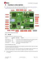
Hardware description
Page 25 of 43
C1-Public
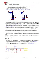
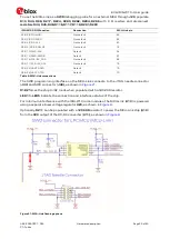
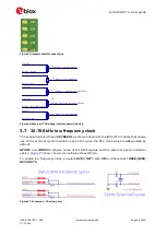
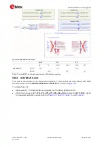
3.8
mikroBUS slots
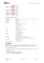
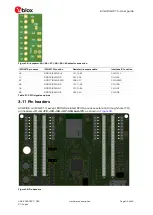
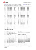
EVK-IRIS-W10 has four mikroBUS standard compatible slots with multiple choices of
RESET
signal for each slot. All slots are not enabled to use by default, and that is mainly due to the
multiplexing of the Flexcomm interfaces pins of the NXP RW612 chip as shown in
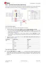
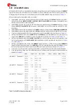
When utilizing the mikroBUS slots, consider:
•
mikroBUS1 cannot be used as SPI interface simultaneously with
WCI-2
function or FTDI-
SPI, which shares
GPIO 0, GPIO 1, GPIO 2, GPIO 3 and GPIO 4
. However, mikroBUS1 can
still be used a UART or I2C interface.
•
mikroBUS2 cannot be used as SPI interface simultaneously with
SDIO
function, which
shares
GPIO 15 and GPIO 16.
However, mikroBUS2 can still be used as a UART or I2C
interface.
•
mikroBUS4 cannot be used totally with
RMII
interface, which shares
GPIO 56 and GPIO 57
.
•
mikroBUS3 cannot be used totally with
JTAG
interface, which shares all GPIOs on this slot.
•
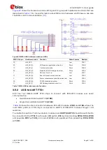
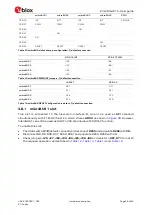
There is a dedicated GPIO for the analog pin in each mikroBUS slot, as shown in
•
All four mikroBUS slots share
GPIO 27
as the
PWM
pin, so this GPIO can only be used in a
single slot.
GPIO 27
is enabled on slot 2 by default, as shown in
•
All four mikroBUS slots share
GPIO 18
as
INT
pin, so this can be used in a single slot – but
not simultaneously with
SDIO. GPIO 18
is enabled on slot 2 by default, as shown in
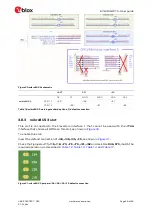
•
All four mikroBUS slots share the
RESET
signal options – either to the global
RESETn
signal of the EVB (active low) or to
GPIO 50
, which is intended as user-defined RESET. This
is mainly because the Click boards have different reset options, as shown in
•
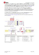
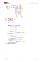
The inner row of each slot is easily accessible – even with the use of add-on Click boards.
•
The top-position slots are for extended use or include antenna add-on Click boards, as
shown in
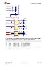
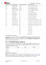
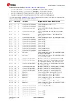
GPIO
UART
SPI
I2C
SDIO
JTAG
WCI-2
RMII
FTDI
mikroBUS 1 Flexcomm 0
GPIO0
CS
SPI-RX
GPIO2
RX
MOSI SDA
SPI-CS
GPIO3
TX
MISO SCL
SPI-TX
GPIO4
CLK
WCI-2
SPI-Clk
mikroBUS 2 Flexcomm 2
GPIO13
RXD
MOSI SDA
GPIO14
TXD
MISO SCL
GPIO15
CLK
SDIO-CLK
GPIO16
CS
SDIO-D3
mikroBUS 3 Flexcomm 1
GPIO6
CS
JTAG
GPIO7
CLK
JTAG
GPIO8
TXD
MISO SCL
JTAG
GPIO9
RXD
MOSI SDA
JTAG
mikroBUS 4 Flexcomm 14
GPIO53
CS
GPIO54
CLK
GPIO56
TXD
MISO SCL
MDC
GPIO57
RXD
MOSI SDA
MDIO
Table 11: mikroBUS slots pin configuration