EVK-NINA-B4 - User guide
UBX-19054587 - R04
Board configuration
Page 17 of 40
C1 - Public
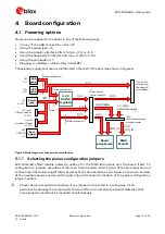
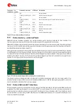
Default power configuration, 3.3 V
This is the default power configuration for the evaluation board, and the jumpers are installed
out-of-the-box with this power configuration. All board peripherals are powered up, the NINA module
is directly supplied by the board, and everything is running at 3.3 V.
Figure 9: Jumper positions for default power configuration
Connector
Add jumper to pins
Description
J7
7, 8
Selects the board regulated 3.3 V net as source for the VDD_NINA net.
9, 10
Powers up the Interface MCU, USB hub, and UART to USB converter with 3.3 V.
J22
1, 3
Powers up the NINA module. The NINA VCC and VCC_IO pins are connected to the
selected source for the VDD_NINA net.
2, 4
Powers up the peripherals directly connected to NINA such as LEDs and external
memory with the NINA supply voltage.
Table 3: Jumper positions for default power configuration
J7
B
O
ARD
NINA
3V3
3
4
2
1
J22
V
C
C
_IO
V
C
C
7
8
9
10
NINA module power
board I/O power
J22: 2-4
J22: 1-3
PC communication
MCU
DC/DC
EVB powered
J7: 9-10
J7: 7-8


