background image


EVK-NINA-B4 - User guide 

UBX-19054587 - R04 

Board configuration


Page 20 of 40 

C1 - Public 


External supply, 3.6

1.7 V 

When  measuring  current  consumption  or  performing  other  NINA-B4  module  characterization 
measurements, it can be useful to power the module with an external source such as a lab power 
supply. In such cases, all jumpers can be removed and the required supply nets can be fed externally 
by connecting to the pin headers. For example, the NINA-B4 module can be powered by connecting an 
external supply directly to the J22 pin 1 and GND. See also 

Using an external power supply or power 

analyzer


Make sure that unpowered parts of the board are properly isolated from the NINA module. If a 
voltage is applied to the signal of an unpowered device/component, current might leak through 
various protection circuits of this device. This might give false readings when measuring current 
consumption. Isolation can be achieved by removing NINA signal jumpers. See also 

Disconnecting NINA signals from board peripherals

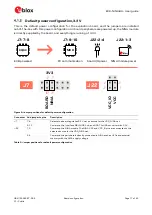
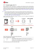
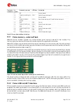
Figure 12 below shows a few optional jumper connections that can be helpful when supplying the 
module with an external supply. 


Figure 12: Optional jumper positions while using an external power supply 

Connector


Add jumper to pins


Description


J7 

7, 8 

(Optional) Selects the board regulated 3.3 V net as a source for the VDD_NINA net. 

9, 10 

(Optional) Powers up the Interface MCU, USB hub, and UART to USB converter with 3.3 V.  

J22 

3, 4 

(Optional) Powers up the peripherals directly connected to NINA such as LEDs and 
external memory with the selected source for the VDD_NINA net. 

Table 6: Optional jumper positions while using an external supply 


J7

B

O

ARD

NINA

3V3

3

4

J22

7

8

9

10

board I/O power

(optional)

J22: multiple

PC communication

(optional)

MCU

DC/DC

EVB powered

(optional)

J7: 9-10

J7: 7-8

V

C

C

_IO

V

C

C

1

2

5

6

GND

-.--   V

External supply

Содержание EVK-NINA-B400

Страница 1: ...User guide Abstract This document describes how to set up the EVK NINA B4 evaluation kit to evaluate NINA B4 series standalone Bluetooth 5 1 low energy modules It also describes the different options...

Страница 2: ...property rights in the products names logos and designs included in this document Copying reproduction modification or disclosure to third parties of this document or any part thereof is only permitt...

Страница 3: ...r analyzer 13 4 Board configuration 14 4 1 Powering options 14 Selecting the power configuration jumpers 14 Default power configuration 3 3 V 17 Battery powered 3 1 7 V 18 Battery powered with protect...

Страница 4: ...EVK NINA B4 User guide UBX 19054587 R04 Contents Page 4 of 40 C1 Public Appendix 34 A Schematics 34 B Glossary 38 Related documents 39 Revision history 39 Contact 40...

Страница 5: ...on from the Windows Start button Install J Link drivers Follow the procedure outlined below to install the J Link drivers needed for programming the module 1 Connect the EVK NINA B4 board to your PC u...

Страница 6: ...PU NINA B400 module and U FL antenna connector for connecting to external antennas The EVK NINA B400 is also used for evaluation of NINA B401 module EVK NINA B410 with u connect NINA B410 module pre f...

Страница 7: ...ors the manufacturer of the nRF52833 SoC provide a free Software Development Kit SDK that includes a broad selection of drivers libraries and example applications that can be used for rapid prototypin...

Страница 8: ...supply o 5 12 V Arduino VIN input Battery holder supporting CR2032 coin cell batteries 2 4 EVK NINA B4 block diagram Figure 3 shows the major interfaces and internal connections of the EVK NINA B4 Fig...

Страница 9: ...the EVK NINA B400 EVK NINA B410 J12 Cortex Debug connector 10 pin 50 mil pitch connector that can be used to connect external debuggers to the NINA B4 module The NINA B4 modules support Serial Wire d...

Страница 10: ...valuation board Center conductor is positive and the ring is negative The operating system installs the correct drivers automatically The drivers need only be installed once when you connect the unit...

Страница 11: ...n about performing these tasks see the Software section of the NINA B4 system integration manual 4 See also the u blox short range open CPU github repository 9 3 2 2 2 Software debug options Use eithe...

Страница 12: ...be measured with a voltmeter To modify the board solder a low resistance high tolerance 0402 sized resistor to the footprint labeled R6 This resistor replaces the jumper normally positioned between J2...

Страница 13: ...r the signal from the NINA module is connected to an EVK peripheral The leakage is typically in the order of 100 s of nano amps To reduce leakage current use a second external power channel to supply...

Страница 14: ...moved to pin headers shorting two of the pins together and connecting or disconnecting different power nets on the evaluation board Figure 7 shows an overview of the available power sources and target...

Страница 15: ...d 3 3 V converter Battery Battery with protection diode MCU PC communication HAT Raspberry Pi expansion board NINA module power Board I O power Level shifters LEDs etc 3V3 VBAT_DIODE VBAT VDD_MCU 3V3_...

Страница 16: ...upplied by the board and will always be powered as long as a power source is connected 8 VDD_NINA Connects to J22 pin 3 from where it can be connected to the module supply pin or somewhere else 9 3V3...

Страница 17: ...ector Add jumper to pins Description J7 7 8 Selects the board regulated 3 3 V net as source for the VDD_NINA net 9 10 Powers up the Interface MCU USB hub and UART to USB converter with 3 3 V J22 1 3 P...

Страница 18: ...an extra board peripheral might deplete the battery Do not connect jumpers J7 5 6 and J7 7 8 at the same time while a battery is connected This might cause damage to the battery Figure 10 Jumper posi...

Страница 19: ...mper positions for battery powered operation with a protection diode dashed lines show optional jumpers Connector Add jumper to pins Description J7 3 4 Selects the diode protected battery as a source...

Страница 20: ...this device This might give false readings when measuring current consumption Isolation can be achieved by removing NINA signal jumpers See also Disconnecting NINA signals from board peripherals Figur...

Страница 21: ...onnected to the selected source for the VDD_NINA net 2 4 Optional Powers up the peripherals directly connected to NINA such as LEDs and external memory with the NINA supply voltage Table 7 Jumper conf...

Страница 22: ...B41 RED signal 12 RED RGB diode red signal active low J9 1 GPIO_16 UART_DTR NINA B40 analog capable GPIO signal NINA B41 UART DTR output 2 UART_DTR_I UART to USB DTR signal 3 GPIO_17 UART_DSR NINA B40...

Страница 23: ...na to the EVK NINA B410DF as described in Table 9 EVK NINA B410DF CoreHW antenna D4 8 ANT_SEL3 D5 6 ANT_SEL2 D8 7 ANT_SEL1 D9 5 ANT_SEL0 D12 or GND 9 GND D13 or 3V3 10 3V3 3V3 1 and 2 GND 3 and 4 Tabl...

Страница 24: ...DS3 Interface MCU LED Blinks on USB enumeration and activity lit when the Interface MCU is connected via USB DS4 Interface MCU LED Error LED DS5 UART DTR LED Connected to the NINA UART_DTR GPIO_16 pin...

Страница 25: ...ected 2 IOREF I O reference voltage level Selectable by user to 1 7 3 6 V VDD_IO See also Selecting the power configuration jumpers 3 RESET NINA reset signal input Active low logic RESET_N P0 18 4 3 3...

Страница 26: ...al on NINA B41 3 D2 Digital I O UART_CTS GPIO_21 P0 23 UART_CTS signal on NINA B41 4 D3 Digital I O UART_RTS GPIO_20 P0 31 UART_RTS signal on NINA B41 5 D4 Digital I O GPIO_1 P0 13 6 D5 Digital I O GP...

Страница 27: ...NINA pin 22 SCL SDA On some Arduino boards the I2C signals SCL and SDA are connected to pins A4 and A5 and to the SCL and SDA pins in the top right hand corner Since these pins will be shorted togethe...

Страница 28: ...y pin 5V Cannot be used as supply input Supplied by USB VBUS and protected from back powering 5 GPIO03 Digital I O GPIO_4 P0 16 6 GND Ground GND GND 7 GPIO04 Digital I O GPIO_3 P0 01 Disconnected by d...

Страница 29: ...floating 19 GPIO10 Digital I O GPIO_48 P0 21 Connected to NINA through a solder bridge if the bridge is cut this pin will be left floating 20 GND Ground GND GND 21 GPIO09 Digital I O GPIO_47 P0 06 Co...

Страница 30: ...is configured to simulate a HAT with GPIO14 connected to the NINA UART_RXD pin and GPIO15 connected to the NINA UART_TXD pin EEPROM support The Raspberry Pi interface supports a unique EEPROM solution...

Страница 31: ...signal 2 MCU_RXD Interface MCU data input signal 3 MCU_RTS Interface MCU flow control output signal 4 MCU_CTS Interface MCU flow control input signal 5 GND GND Ground J21 1 VDD_IO Supply net for LEDs...

Страница 32: ...s Data sheet 1 SPI signals are shared with other interfaces and GPIO functions and are routed to the GPIO pin header J14 Raspberry Pi interface and flash memory footprint on the bottom side of the eva...

Страница 33: ...50 mil pitch Cortex Debug ETM connector This extended connector has the same features as J12 but also accommodates instruction trace operations through the Embedded Trace Macrocell ETM of the Cortex...

Страница 34: ...EVK NINA B4 User guide UBX 19054587 R04 Appendix Page 34 of 40 C1 Public Appendix A Schematics...

Страница 35: ...EVK NINA B4 User guide UBX 19054587 R04 Appendix Page 35 of 40 C1 Public...

Страница 36: ...EVK NINA B4 User guide UBX 19054587 R04 Appendix Page 36 of 40 C1 Public For the first prototype build marked PT1 EVK NINA B3 schematic can be used as a reference...

Страница 37: ...4 User guide UBX 19054587 R04 Appendix Page 37 of 40 C1 Public For the first prototype build marked PT1 EVK NINA B3 schematic can be used as a reference Pages 2 and 6 of the schematic are intentionall...

Страница 38: ...eral Purpose Input Output LED Light Emitting Diode MCU Micro controller unit MSD Mass storage device NFC Near Field Communication U FL Coaxial RF connector USB Universal serial bus RTS Request To send...

Страница 39: ...com u blox u blox sho OpenCPU 10 CoreHW https www corehw com For product change notifications and regular updates of u blox documentation register on our website www u blox com Revision history Revis...

Страница 40: ...onal Office China Beijing Phone 86 10 68 133 545 E mail info_cn u blox com Support support_cn u blox com Regional Office China Chongqing Phone 86 23 6815 1588 E mail info_cn u blox com Support support...

Страница 41: ...FWM7BLZ20 EB KIT SP14801 DUT SKY66111 21EK1 SECO RSL10 TAG GEVB 3026 MIKROE 2471 BLE IOT GEVB 450 0184 EKSHCNZXZ EVAL_PAN1026 EVAL_PAN1720 EVAL_PAN1740 2267 2479 2487 2633 STEVAL IDB005V1D STEVAL IDB0...

Отзывы: