EVK-JODY-W3 - User guide
UBX-20030840 - R02
Board description
Page 12 of 29
4
Board description
This section describes the logical components, connectors, jumpers and switches used to configure
the EVK-JODY-W3.
4.1
Block diagram
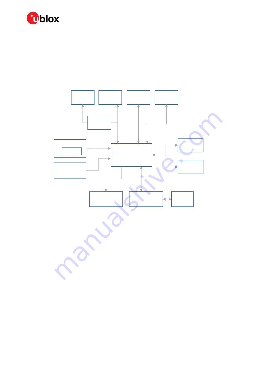
Figure 4 shows the block diagram of the EVK with the different peripheral connectors around it.
Figure 4: EVK-JODY-W3 block diagram
4.2
Overview of jumpers and connectors
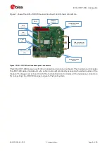
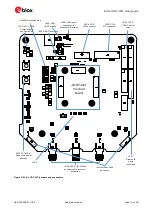
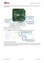
Figure 5 shows an overview of the evaluation board and its connectors. The EVK makes all the
interfaces of the JODY-W3 series module accessible through connectors or pin headers. The available
interfaces and configurations options are described in detail in the following sections.
JODY-W3
module
2x internal
dual-band
t
3x SMA
connector
Control lines
and GPIOs
Audio interface
(PCM/I2S)
PCIe
interface
UART
interface
USB
interface
UART to
USB
Power supply
SDIO
interface
DC-DC
Bootstrap
configuration
Audio
codec

