background image

Input Configuration

1-5

General Information

1.3

Input Configuration

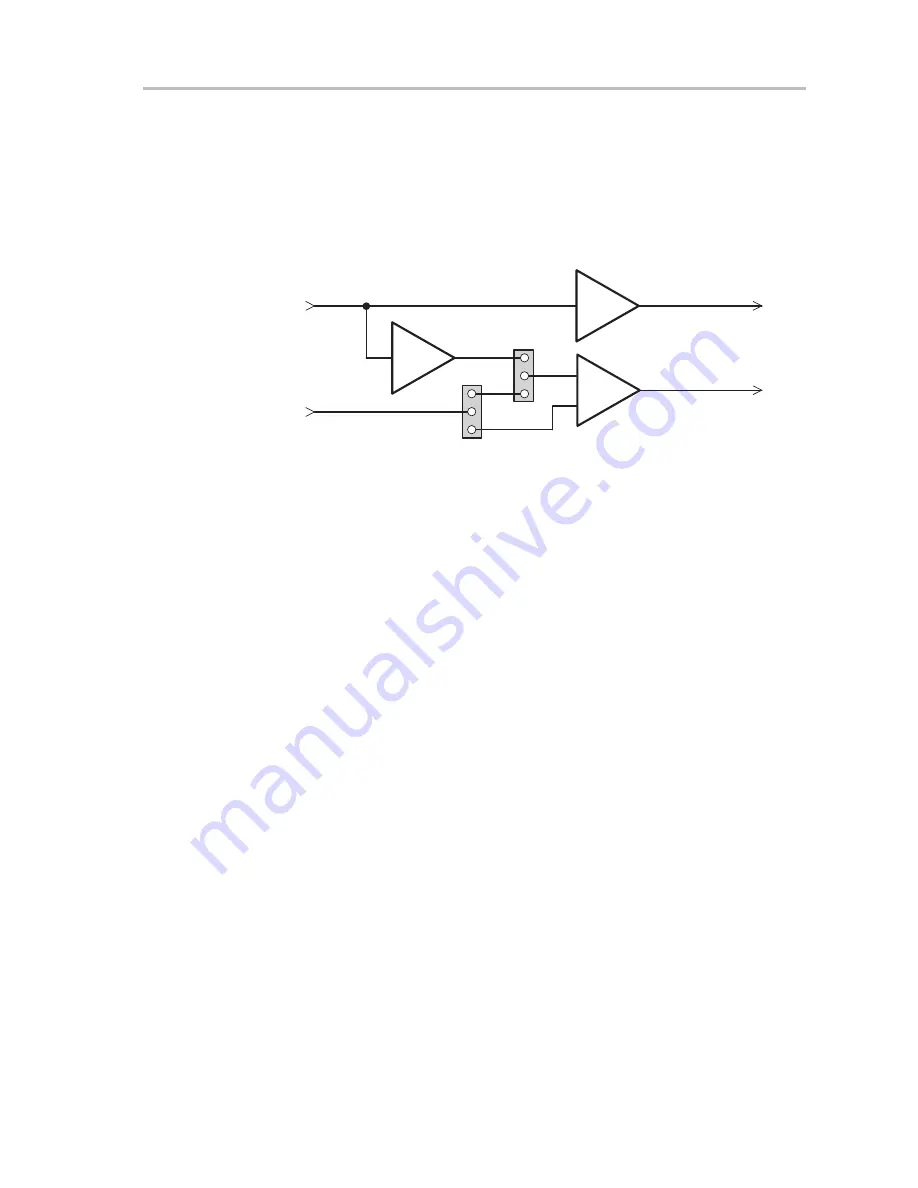
The THS6022 EVM inputs can be configured in several different ways to
provide a wide variety of circuits to support different applications
(Figure 1–3). Each of the two jumpers on the EVM is a three-pin header that
is used as a SPDT switch by placing a shunt across two pins to select either
of two possible signal routes.

Figure 1–3. THS6022 Evaluation Module Block Diagram

J4

1

3

2

JP1

1

3

2

JP2

+

J6

THS6022

THS6022

THS4001

U1

U2: A

U2: B

Driver 1 Output

Driver 2 Output

Driver 1

Input

Driver 2

Input

Positive Driver

Inverter

Negative Driver

J5

J7

-

Jumper JP1:

J

1–2 — connects the noninverting input of driver 2 (U2: B) to the
THS4001 inverting amplifier (U1) output

J

2–3 — connects the noninverting input of driver 2 (U2: B) to the input
connector (J6) when jumper JP2 is set appropriately

-

Jumper JP2:

J

1–2 — connects the driver 2 input connector (J6) to the noninverting
input of driver 2 (U2:B) when jumper JP1 is set appropriately

J

2–3 — connects the driver 2 input connector (J6) to the inverting input
of driver 2 (U2:B) when jumper JP1 is set appropriately

For example, to use a single-ended input, jumper JP1 should be set to 1–2 and
the input signal applied to input connector J4. The output of the THS6022
drivers is a differential signal due to the inverter (U1) and JP1 being set to 1–2.
For a differential source, JP1 should be set to 2–3, JP2 should be set to 1–2
and the differential input signal applied between input connectors J4 and J6.

If JP2 is in the 2–3 position, components C12 and R11 must be installed, R9
must be removed, and a 0-

 resistor must be installed in the C11 position for

proper operation.

1.4

THS6022 EVM Specifications

Supply voltage range, 

±

V

CC

±

5 V to 

±

15 V

. . . . . . . . . . . . . . . . . . . . . . . . . . . . . . . . . . . . . . . . . . . . 

Supply current, I

CC 

23 mA

. . . . . . . . . . . . . . . . . . . . . . . . . . . . . . . . . . . . . . . . . . . . . . . . . . . . . . . . . . . 

Input voltage, V

±

V

CC

, max

. . . . . . . . . . . . . . . . . . . . . . . . . . . . . . . . . . . . . . . . . . . . . . . . . . . . . . . . . 

Output drive, THS6022 Drivers, I

250 mA, typ each

. . . . . . . . . . . . . . . . . . . . . . . . . . . . . . . . . . . . 

Continuous total power dissipation at TA = 25

°

C (THS6022),

3.3 W, max

. . . . . . . . . . . . . . . . . . . 

For complete THS6022 amplifier IC specifications and parameter
measurement information, and additional application information, see the
THS6022 data sheet, TI Literature Number SLOS225.

Содержание ths6022

Страница 1: ...THS6022 250ĆmA Dual Differential Drivers Evaluation Module November 1998 Mixed Signal Products User s Guide SLOU035 ...

Страница 2: ...CONDUCTOR PRODUCTS MAY INVOLVE POTENTIAL RISKS OF DEATH PERSONAL INJURY OR SEVERE PROPERTY OR ENVIRONMENTAL DAMAGE CRITICAL APPLICATIONS TI SEMICONDUCTOR PRODUCTS ARE NOT DESIGNED AUTHORIZED OR WARRANTED TO BE SUITABLE FOR USE IN LIFE SUPPORT DEVICES OR SYSTEMS OR OTHER CRITICAL APPLICATIONS INCLUSION OF TI PRODUCTS IN SUCH APPLICATIONS IS UNDERSTOOD TO BE FULLY AT THE CUSTOMER S RISK In order to ...

Страница 3: ...cial PowerPAD package in which the THS6022 amplifier IC is supplied FCC Warning This equipment is intended for use in a laboratory test environment only It generates uses and can radiate radio frequency energy and has not been tested for compliance with the limits of computing devices pursuant to subpart J of part 15 of FCC rules which are designed to provide reasonable protection against radio fr...

Страница 4: ...iv ...

Страница 5: ... 1 3 Input Configuration 1 5 1 4 THS6022 EVM Specifications 1 5 1 5 Using The THS6022 EVM 1 6 1 6 THS6022 EVM Performance 1 7 1 7 General High Speed Amplifier Design Considerations 1 8 1 8 General PowerPAD Design Considerations 1 9 2 Reference 2 1 2 1 THS6022 Dual Differential Line Drivers EVM Parts List 2 2 2 2 THS6022 EVM Board Layouts 2 3 ...

Страница 6: ... W Load 1 7 1 5 THS6022 EVM Driver Frequency Response Test Circuit 1 7 1 6 PowerPAD PCB Etch and Via Pattern Minimum Requirements 1 9 1 7 Maximum Power Dissipation vs Free Air Temperature 1 10 2 1 THS6022 EVM Component Placement Silkscreen and Layout 2 3 2 2 THS6022 EVM PC Board Layer 1 Top Side Layout 2 3 2 3 THS6022 EVM PC Board Layer 2 Back Side Ground Plane Layer 2 4 2 4 THS6022 EVM PC Board S...

Страница 7: ...nd schematic diagrams EVM specifications details on configuring connecting and using the EVM and a discussion on high speed amplifier and PowerPAD package design considerations Topic Page 1 1 Features 1 2 1 2 Description 1 2 1 3 Input Configuration 1 5 1 4 THS6022 EVM Specifications 1 5 1 5 Using The THS6022 EVM 1 6 1 6 THS6022 EVM Performance 1 7 1 7 General High Speed Amplifier Design Considerat...

Страница 8: ...e EVM is a complete client side ADSL high speed driver circuit It consists of the TI THS6022 Dual Differential Line Driver IC a TI THS4001 High Speed Low Power Operational Amplifier IC and a number of passive parts all mounted on a multilayer circuit board Figure 1 1 The EVM uses standard BNC connectors for inputs and outputs and also includes a pad area for user component connection and testing I...

Страница 9: ... 5 4 R4 1 KΩ R2 49 9 Ω R3 1 KΩ R1 49 9 Ω R8 49 9 Ω R7 TBD 15 V 15 V R5 1 KΩ 15 V 6 4 7 15 V 2 3 JP1 JP2 R9 49 9 Ω 13 14 12 10 11 R11 TBD U2 B THS6022 15 V R15 49 9 Ω R14 TBD R12 1 KΩ R13 1 KΩ C4 TBD C13 0 1 µF C3 0 1 µF C2 0 1 µF C6 TBD R6 1 KΩ U1 THS4001 C7 0 1 µF C5 0 1 µF C12 TBD C10 0 1 µF C9 0 1 µF C14 0 1 µF C11 TBD J4 Driver 1 Input 1 J6 Driver 2 Input R10 49 9 Ω 15 V J5 Driver 1 Output Dri...

Страница 10: ...s Any of the components on the EVM board can be replaced with different values Also component pads have been placed in convenient locations on the PCB shown as components with the value TBD in the schematic to allow numerous modifications to the basic EVM configuration However care must be taken because the surface mount solder pads on the board are somewhat fragile and will not survive a large nu...

Страница 11: ...r 2 U2 B when jumper JP1 is set appropriately J 2 3 connects the driver 2 input connector J6 to the inverting input of driver 2 U2 B when jumper JP1 is set appropriately For example to use a single ended input jumper JP1 should be set to 1 2 and the input signal applied to input connector J4 The output of the THS6022 drivers is a differential signal due to the inverter U1 and JP1 being set to 1 2 ...

Страница 12: ...er 1 amplifier output Connecting directly to the DRIVER 1 OUTPUT BNC connector J5 with a 50 Ω nominal impedance cable and an oscilloscope having a 50 Ω input termination is preferred for examining very high frequency signals 5 Set jumper J1 to the 1 2 position 6 Set jumper J2 to the 1 2 position 7 Set the power supply to ON 8 Connect a signal input to the DRIVER 1 INPUT BNC J4 Each input connector...

Страница 13: ...haracteristics of the inverting amplifier U1 Component values can be changed to cause the two responses to track more closely but since ADSL signals are limited to 2 MHz and below the high frequency imbalance can usually be ignored Figure 1 4 THS6022 EVM Driver Frequency Response With a 50 Ω Load f Frequency Hz OUTPUT LEVEL vs FREQUENCY 1 3 10M 100k 1 3 500M Output Level dB 5 7 1M 100M VCC 5V VI P...

Страница 14: ...pins can seriously degrade the performance of the amplifiers In addition ground plane coupling into these pins can cause noise to appear at the outputs of the amplifiers This is especially important for the inverting pin while the amplifier is operating in the noninverting mode Because the voltage at this pin swings directly with the noninverting input voltage any stray capacitance would allow cur...

Страница 15: ...ese holes should be 13 mils in diameter They are kept small so that solder wicking through the holes is not a problem during reflow 3 Additional vias may be placed anywhere along the thermal plane outside of the thermal pad area This will help dissipate the heat generated from the THS6022 These additional vias may be larger than the 13 mil diame ter vias directly under the thermal pad They can be ...

Страница 16: ...hen the expected thermal coefficient θJA is about 37 5_C W For a given θJA the maximum power dissipation is shown in Figure 1 7 and is calculated by the following formula P D ǒT MAX T A qJA Ǔ Where PD Maximum power dissipation of THS6022 watts TMAX Absolute maximum junction temperature 150 C TA Free ambient air temperature C θJA θJC θCA θJC Thermal coefficient from junction to case 2 07 C W θCA Th...

Страница 17: ... is a good example of proper thermal management when using PowerPAD mounted devices Correct PCB layout and manufacturing techniques are critical for achieving adequate transfer of heat away from the PowerPAD IC package More details on proper board layout can be found in the THS6022 250 mA DUAL DIFFERENTIAL LINE DRIVER data sheet SLOS225 For more general information on the PowerPAD package and its ...

Страница 18: ...1 12 General Information ...

Страница 19: ...ce Reference This chapter includes a parts list and PCB layout illustrations for the THS6022 EVM Topic Page 2 1 THS6022 Dual Differential Line Drivers EVM Parts List 2 2 2 2 THS6022 EVM Board Layouts 2 3 Chapter 2 ...

Страница 20: ...MOUSER 523 31 5329 J1 J2 J3 JACK BANANA RECEPTANCE FOR 0 25 DIA HOLE 2 JP1 JP2 HEADER 3 PIN 0 1 CTRS 0 025 SQ PINS 2 R2 R9 RESISTOR 49 9 OHMS 1 10W 1 SM 0805 2 R1 R8 R10 R15 RESISTOR 49 9 OHMS 1 8W 1 SM 1206 6 R3 R4 R5 R6 R12 R13 RESISTOR 1 K OHM 1 10W 1 SM 0805 6 U2 IC THS6022CPWP 1 TI THS6022CPWP U1 IC OP AMP THS4001CD SOIC 8 1 TI THS4001CD R7 R14 RESISTOR X OHMS 1 8W 1 SM 1206 2 R11 RESISTOR X ...

Страница 21: ... a reference Figure 2 1 THS6022 EVM Component Placement Silkscreen and Layout J2 VCC GND J1 C8 U1 Driver 1 Output L2 Texas Instruments THS6022 EVM SLOP133 Rev B J3 Driver 1 Input J4 R5 R6 L1 C1 R1 R2 J5 U2 R3 JP2 C10 R12 Driver 2 Output Pad1 GND Pad2 C3 R4 C7 Driver 2 Input J6 JP1 R9 R10 J7 C5 R8 C2 C9 R13 R15 C6 C4 R7 C11 R14 C12 R11C14 C13 VCC Figure 2 2 THS6022 EVM PC Board Layer 1 Top Side Lay...

Страница 22: ...THS6022 EVM Board Layouts 2 4 Reference Figure 2 3 THS6022 EVM PC Board Layer 2 Back Side Ground Plane Layer Figure 2 4 THS6022 EVM PC Board Solder Mask Back Side ...

Отзывы: