


SNAS605AR – MARCH 2013 – REVISED DECEMBER 2015
Feature Description (continued)
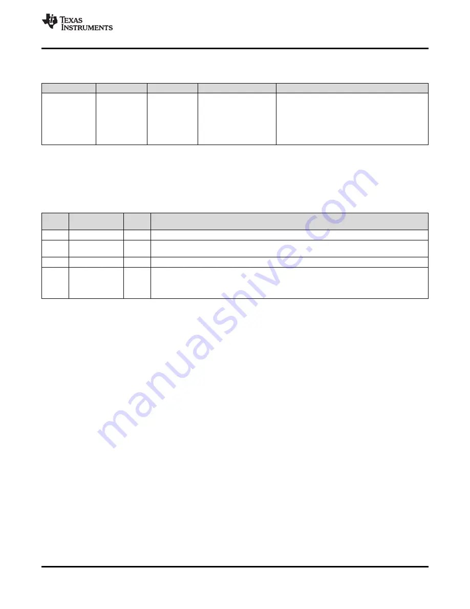
Table 1. Some Possible SYNC Configurations (continued)
NAME
SYNC_MODE
SYSREF_MUX
OTHER
DESCRIPTION
CLKin0_OUT_MUX = 0
SDCLKoutY_DDLY = 0
(Local sysref DDLY
Direct SYSREF
A direct fan-out of SYSREF with no re-clocking to
0
0
bypassed)
distribution
clock distribution path.
SYSREF_DDLY_PD = 1
SYSREF_PLSR_PD = 1
SYSREF_PD = 1.
9.3.2 JEDEC JESD204B
9.3.2.1 How To Enable SYSREF
summarizes the bits needed to make SYSREF functionality operational.
Table 2. SYSREF Bits
REGIS
FIELD
VALUE
DESCRIPTION
TER
0x140
SYSREF_PD
0
Must be clear, power-up SYSREF circuitry.
SYSREF_DDLY_
0x140
0
Must be clear to power-up digital delay circuitry during initial SYNC to ensure deterministic timing.
PD
0x143
SYNC_EN
1
Must be set, enable SYNC.
Do not hold local SYSREF DDLY block in reset except at start.
Anytime SYSREF_PD = 1 because of user programming or device RESET, it is necessary to set
0x143
SYSREF_CLR
1
→
0
SYSREF_CLR for 15 VCO clock cycles to clear the local SYSREF digital delay. Once cleared,
SYSREF_CLR must be cleared to allow SYSREF to operate.
Enabling JESD204B operation involves synchronizing all the clock dividers with the SYSREF divder, then
configuring the actual SYSREF functionality.
9.3.2.1.1
Setup of SYSREF Example
The following procedure is a programming example for a system which is to operate with a 3000 MHz VCO
frequency. Use DCLKout0 and DCLKout2 to drive converters at 1500 MHz. Use DCLKout4 to drive an FPGA at
150 MHz. Synchronize the converters and FPGA using a two SYSREF pulses at 10 MHz.
1.
Program registers 0x000 to 0x1fff as desired. Key to prepare for SYSREF operations:
(a) Prepare for manual SYNC: SYNC_POL = 0, SYNC_MODE = 1, SYSREF_MUX = 0
(b) Setup output dividers as per example: DCLKout0_DIV and DCLKout2_DIV = 2 for frequency of 1500
MHz. DCLKout4_DIV = 20 for frequency of 150 MHz.
(c) Setup output dividers as per example: SYSREF_DIV = 300 for 10 MHz SYSREF
(d) Setup
SYSREF:
SYSREF_PD
=
0,
SYSREF_DDLY_PD
=
0,
DCLKout0_DDLY_PD
=
0,
DCLKout2_DDLY_PD = 0, DCLKout4_DDLY_PD = 0, SYNC_EN = 1, SYSREF_PLSR_PD = 0,
SYSREF_PULSE_CNT = 1 (2 pulses). SDCLKout1_PD = 0, SDCLKout3_PD = 0
(e) Clear Local SYSREF DDLY: SYSREF_CLR = 1.
2.
Establish deterministic phase relationships between SYSREF and Device Clock for JESD204B:
(a) Set device clock and SYSREF divider digital delays: DCLKout0_DDLY_CNTH, DCLKout0_DDLY_CNTL,
DCLKout2_DDLY_CNTH, DCLKout2_DDLY_CNTL, DCLKout4_DDLY_CNTH, DCLKout4_DDLY_CNTL,
SYSREF_DDLY.
(b) Set device clock digital delay half steps: DCLKout0_HS, DCLKout2_HS, DCLKout4_HS.
(c) Set SYSREF clock digital delay as required to achieve known phase relationships: SDCLKout1_DDLY,
SDCLKout3_DDLY, SDCLKout5_DDLY.
(d) To allow SYNC to effect dividers: SYNC_DIS0 = 0, SYNC_DIS2 = 0, SYNC_DIS4 = 0,
SYNC_DISSYSREF = 0
(e)
Perform SYNC by toggling SYNC_POL = 1 then SYNC_POL = 0.
Copyright © 2013–2015, Texas Instruments Incorporated
37
Product Folder Links: