


Test Setup
www.ti.com
10
SNVU552 – March 2017
Submit Documentation Feedback
Copyright © 2017, Texas Instruments Incorporated
Using the LMG1205HBEVM GaN Half-Bridge Power Stage EVM
5.2
List of Test Points
The test points for switching voltage signals on this EVM have been designed for use with oscilloscope
probes with the included spring-type ground connections (often called pigtails). Using the small pigtails
instead of the ground clips will minimize measurement error and produce a cleaner signal with the fast
switching GaN devices used on this EVM. Refer to
Figure 4
through
Figure 9
to see the intended probe
usage for each of the switching signals. The switching voltage data shown in this user guide has been
obtained using such a measurement method.
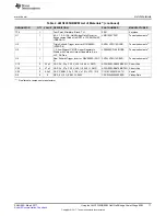
Table 2. Test Point Functional Descriptions
TEST POINT
NAME
DESCRIPTION
TP1
5V_VDD
5-V VDD onboard generated supply
TP2
GND
GND
TP3
HO
High-side GaN FET gate signal
TP4
HB
High-side Floating Bias Supply
TP5
Vbus sense +
High-sense connection for Vbus input voltage
TP6
Vbus sense –
Low-sense connection for Vbus input voltage (PGND)
TP7
Vout sense +
High-sense connection for Vout output voltage
TP8
HI
High-side GaN FET control input signal
TP9
LI
Low-side GaN FET control input signal
TP10
Vout sense –
Low-sense connection for Vbus output voltage (PGND)
TP11
LO
Low-side GaN FET gate signal
TP12
HS
High-side GaN FET source signal (that is, SW node)
J5
Iout sense
Output current sense through 5-m
Ω
shunt resistor (1V:20A)
Figure 4. HI Test Point (TP8)
Figure 5. LI Test Point (TP9)
Figure 6. HS Test Point (TP12)
Figure 7. HB Test Point (TP4)
Figure 8. HO Test Point (TP3)
Figure 9. LO Test Point (TP11)


