Hardware Description and Setup
2
SNLU222B – December 2016 – Revised September 2019
Copyright © 2016–2019, Texas Instruments Incorporated
FPC401 and FPC402 Evaluation Module (EVM) User’s Guide
1
Hardware Description and Setup
The general procedure for setting up the FPC401 and FPC402 Evaluation Modules (EVM) is described in
the following sections.
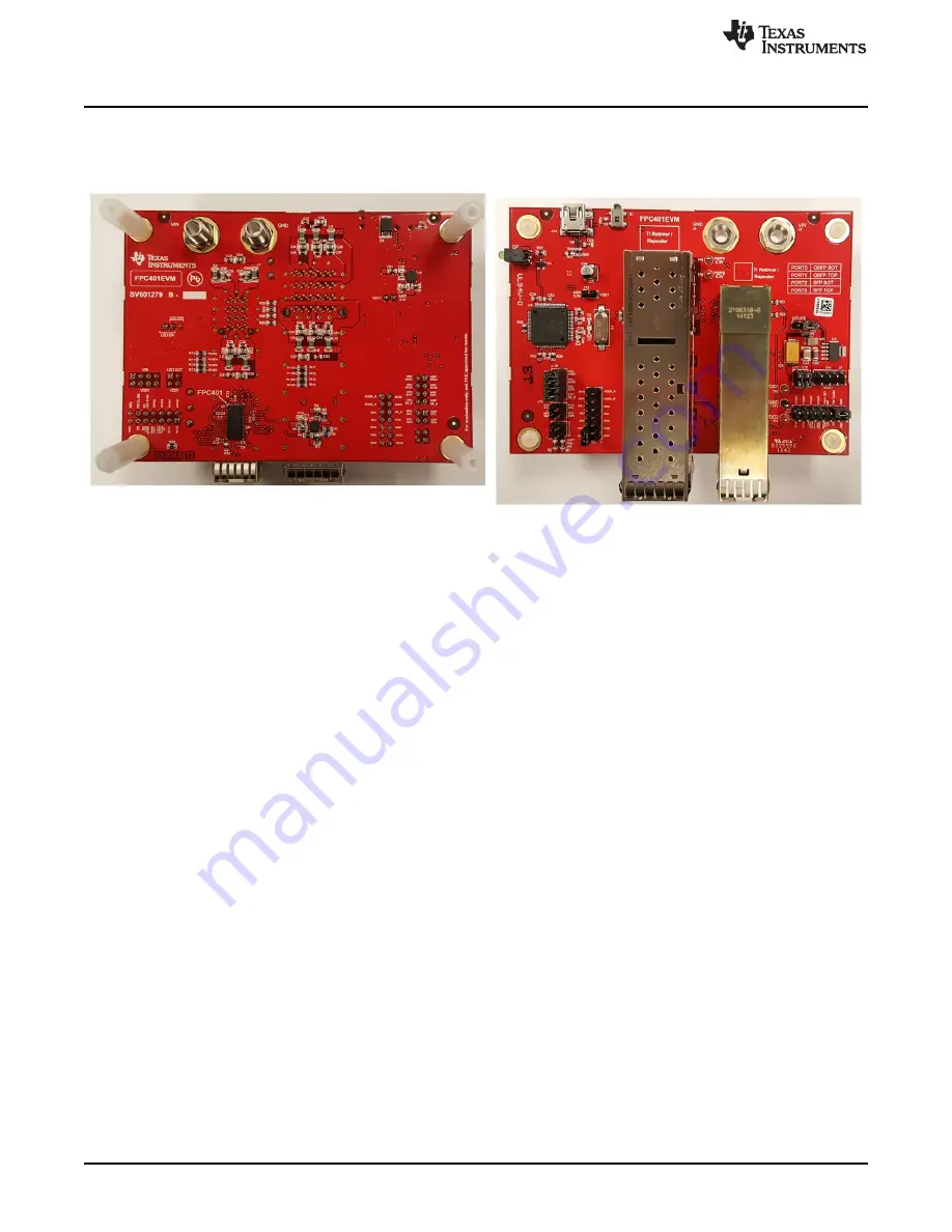
Figure 1. FPC40xEVM – Top and Bottom
1.1
Power Configuration
Configure the power illustrated by
1. If the LDO is used to power the FPC, enable the LDO through header J8 and connect the LDO output
to VDD1 using header J4 (note that each header connection is rated for 1 A of current). Make sure
headers J7 and J13 are disconnected. The LDO has a maximum rated current of 1.5 A, so if the
cumulative QSFP/SFP module current draw is greater than that, the LDO may not be used.
2. If the LDO is not used and the FPC is powered through an external supply, configure the J8 header to
disable the LDO and connect VIN to VDD1 using header J7 (note that each header connection is rated
for 1 A of current). Make sure headers J4 and J13 are disconnected.
3. If USB power is used to power the FPC, ensure the LDO and VIN and disconnected from VDD1
(disconnect headers J4 and J7). Connect the 3.3 V of the MSP430 microcontroller to VDD1 through
header J13. Note that a typical computer USB port is only able to supply up to 100 mA which will be
enough to power the FPC and passive modules (that is, DAC); but it will not be enough to power active
SFP+ and QSFP+ modules which are plugged in.
4. To set VDD2 to 3.3 V, connect it to VDD1 through header J2. To operate at lower host-side supply
voltages (down to 1.8 V), connect an external supply to the header or test point loop (TP3).
5. The FPC401EVM and FPC402EVM includes a TPS2561 power switch which is used to selectively
enable and disable 3.3-V power to the SFP and QSFP ports. The FPC controls this power switch with
its GPIO pins. To supply power to ports 0 and 1 (QSFP+ ports and LEDs), configure the FPC GPIO0
high logic output to enable the power switch. Similarly, configure GPIO1 to high logic to enable power
for ports 2 and 3 (SFP+ ports and LEDs). Alternatively, supply 3.3 V externally through the test points
(TP4 and TP5). Note that the ground is shared with the board.
6. GPIO2 and GPIO3 are connected to the fault outputs of the power switch, and hence should be set as
inputs or left unconfigured.


