10.0k
R16
VCC
VCC
VCC
TP1
TP2
TP3
TRIG
2
OUT
3
RST
4
CVOLT
5
THR
6
DIS
7
+VCC
8
GND
1
U4
TLC555
U
PWM_Duty
U
U
GND
1
2
3
4
5
6
7
8
9
10
P4
5103308-1
W
FGS_CNTL
V
W
W
SCLK
SDATA
V
V
GND
0.01µF
C7
GND
0.01µF
C8
0.1µF
C9
555 Timer as PWM Generator ~25kHz
5K
R17
4
1
2
3
P3
TP7
V_TESTMODE
VCC
TP4
TP6
V3P3
PowerIn
VCC
10µF
C4
10µH
L1
V3P3
4.7µF
C1
10µF
C2
10µF
C3
47µF
C5
V3P3
4.7k
R9
PWM
100
R12
2
1
3
S2
V_TESTMODE
VCC
V3P3
SCLK
1.00k
R1
3.01k
R2
3.01k
R3
PWM_Duty
S2-1: I2C communication with GUI
0.1µF
C6
S2-3:
PWM duty cycle for speed control using POT
PowerIn plus test mode entry
voltage Power
GND
TP8
TP9
TP11
TP12
TP13
TP14
LED1
LED2
LED3
5
4
1
2
3
6
7
8
9
10
11
P2
5
4
1
2
3
6
7
8
9
10
11
P1
FR
PWM
FGS
FG
TOSC
2
1
3
S1
D1
D2
Interface Connectors for Daughter Board
Test Points for GND
USB to Any Connector
V_TESTMODE
10.0k
R4
3
1
2
Q1
1.00k
R5
TOSC
Q2
10.0k
R6
4.7k
R7
J1
V3P3
10.0k
R8
Q3
1.00k
R11
FGS
FGS_CNTL
Q4
10.0k
R13
4.7k
R14
J3
V3P3
4.7k
R10
FR_BUF
FR_BUF
Must have a single point for bidirectional
MBRM110L
TP16
SDATA
FR
100
R15
FG_BUF
FG_BUF
FG
J2
2
4
5
3
U2
2
4
5
3
U3
Speed Control Section
For Factory Testing
I2C Communication
V TestMode= 6.2Volt
Vcc=5Volt
To Enable OTP programming Test Voltage
V3P3
VI
1
GND
2
EN
3
FB
4
SW
5
U1
TPS62203DBV
Schematic and Bill of Materials
7
Schematic and Bill of Materials
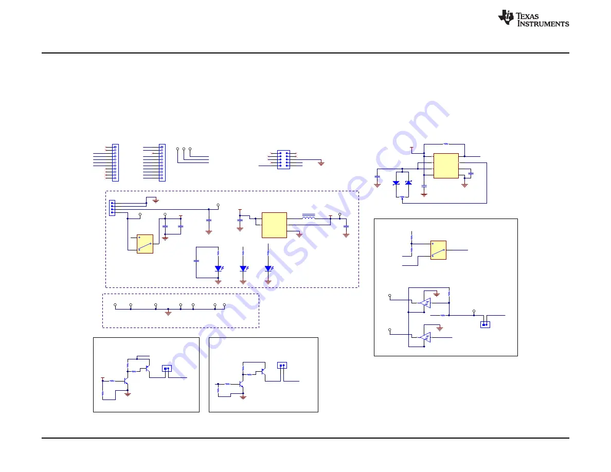
This section contains the DRV10983 schematic and bill of materials (BOM).
7.1
Schematic
shows the DRV10963 motherboard schematic.
Figure 22. DRV10963 Motherboard Schematic
20
DRV10963 Evaluation Module
SLAU643 – July 2015
Copyright © 2015, Texas Instruments Incorporated


