


TMPE627 User Manual Issue 1.0.2
Page 18 of 34
DAC Interface
4.8
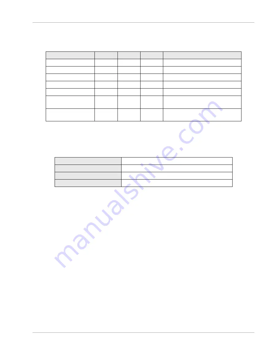
The DAC signals are accessible through the I/O bank 15 of the Artix-7 FPGA.
Signal
Bank
V
CCO
Pin
Description
SCLK
15
3.3 V
F17
Serial Clock Input
SDIN
15
3.3 V
C11
Serial Data Input
SDO
15
3.3 V
A15
Serial Data Output
SYNC#
15
3.3 V
D10
Frame synchronization signal
LDAC#
15
3.3 V
G14
Load DAC
CLR#
15
3.3 V
F14
Sets the DAC registers to zero-
scale or midscale code
BIN2S
15
3.3 V
B15
DAC coding for a bipolar output
range
Table 4-16: DAC I/O Interface
4.8.1 DAC
All analog outputs are directly connected to DAC pins.
Protection
3.5 kV ESD HMB rating on analog input channels
DC Output Impedance
0.5
Ω
Load
2 k
Ω
Capacitive Load
4000 pF
Table 4-17: DAC Electrical Interface
4.8.2 DAC Overcurrent Protection
Generally the DAC’s “Automatic Channel Power-Down” overcurrent protection feature should be used
instead of the current limit clamp. This minimizes the effect of a fault on a DAC output because of the limited
power supply.
In case of an overload condition, the DAC channel is powered down and its output is clamped to ground with
a resistance of ~4 k
Ω. This condition is indicated by the OCx bit set to ‘1’ and the PUx set to ‘0’. The channel
can be powered up again by setting the PUx bit back to ‘1’ after the overload condition is relieved.


