Apollo Carrier Board
User Manual
44
www.terasic.com
September 22, 2020
FPGA Application Design
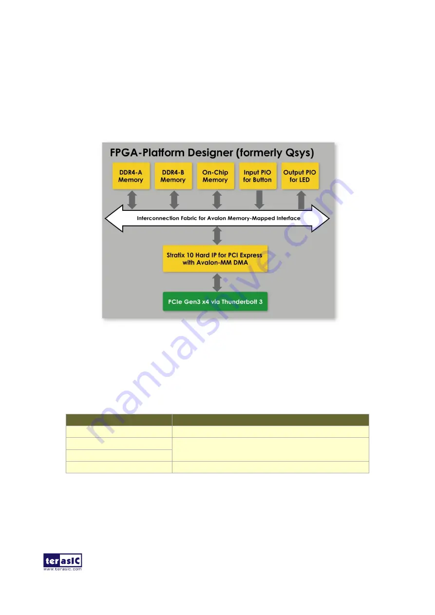
shows the system block diagram in the FPGA system. In the
Platform Designer
(formerly Qsys), the PIO controller is used to control the LED and monitor the Button Status, and
the On-Chip memory is used for performing DMA testing. The PIO controllers and the On-Chip
memory are connected to the PCI Express Hard IP controller through the Memory-Mapped
Interface.
Figure 5-15
Hardware block diagram of the PCIe_DDR4 reference design
Windows Based Application Software Design
The application software project is built by Visual C++ 2012. The project includes the following
major files:
Name
Description
PCIE_DDR4.cpp
Main program
PCIE.c
Implement dynamically load for
TERAISC_PCIE_AVMM.DLL
PCIE.h
TERASIC_PCIE_AVMM.h
SDK library file, defines constant and data structure
The main program PCIE_DDR4.cpp includes the header file "PCIE.h" and defines the controller
address according to the FPGA design.


