background image

March 2017

DocID029088 Rev 3

1/80

1

UM2036


User manual

Evaluation board with STM32F779NI MCU

Introduction

The STM32F779I-EVAL evaluation board is a complete demonstration and development 
platform for STMicroelectronics ARM

®

 Cortex

®

-M7 core-based STM32F779NI 

microcontrollers. It features the following interfaces: four I

2

Cs, six SPIs with three 

multiplexed full-duplex I

2

S, SDIO, two SAIs, 8-bit to 14-bit digital camera, Ethernet MAC, 

FMC, Quad-SPI. It also features four USARTs and four UART peripherals, two CAN buses, 
three 12-bit ADC converters, two 12-bit DAC channels, internal 512 Kbytes of SRAM + 16 
Kbytes of instruction, 2 Mbytes of Flash memory, TCM RAM + 4 Kbytes of backup SRAM, 
USB OTG HS and USB OTG FS peripherals, SWD and JTAG debugging support, 
Cryptographic acceleration (hardware acceleration for AES 128, 192, 256, triple DES, 
HASH (MD5, SHA-1, SHA-2), and HMAC). This evaluation board can be used as a 
reference design for user application development but it is not considered as a final 
application.

The full range of hardware features on the board helps the user to evaluate all the 
peripherals (USB OTG HS, USB OTG FS, Ethernet, motor control, microSD

 card, USART, 

audio DAC and ADC, digital microphone, CAN, SRAM, NOR Flash, SDRAM, Quad SPI 
Flash, 4" DSI LCD with capacitive touch panel etc.) and develop applications. Extension 
headers make provide an easy mean of connecting a daughterboard for a specific 
application.The integrated ST-LINK/V2-1 provides an embedded in-circuit debugger and 
programmer for the STM32.

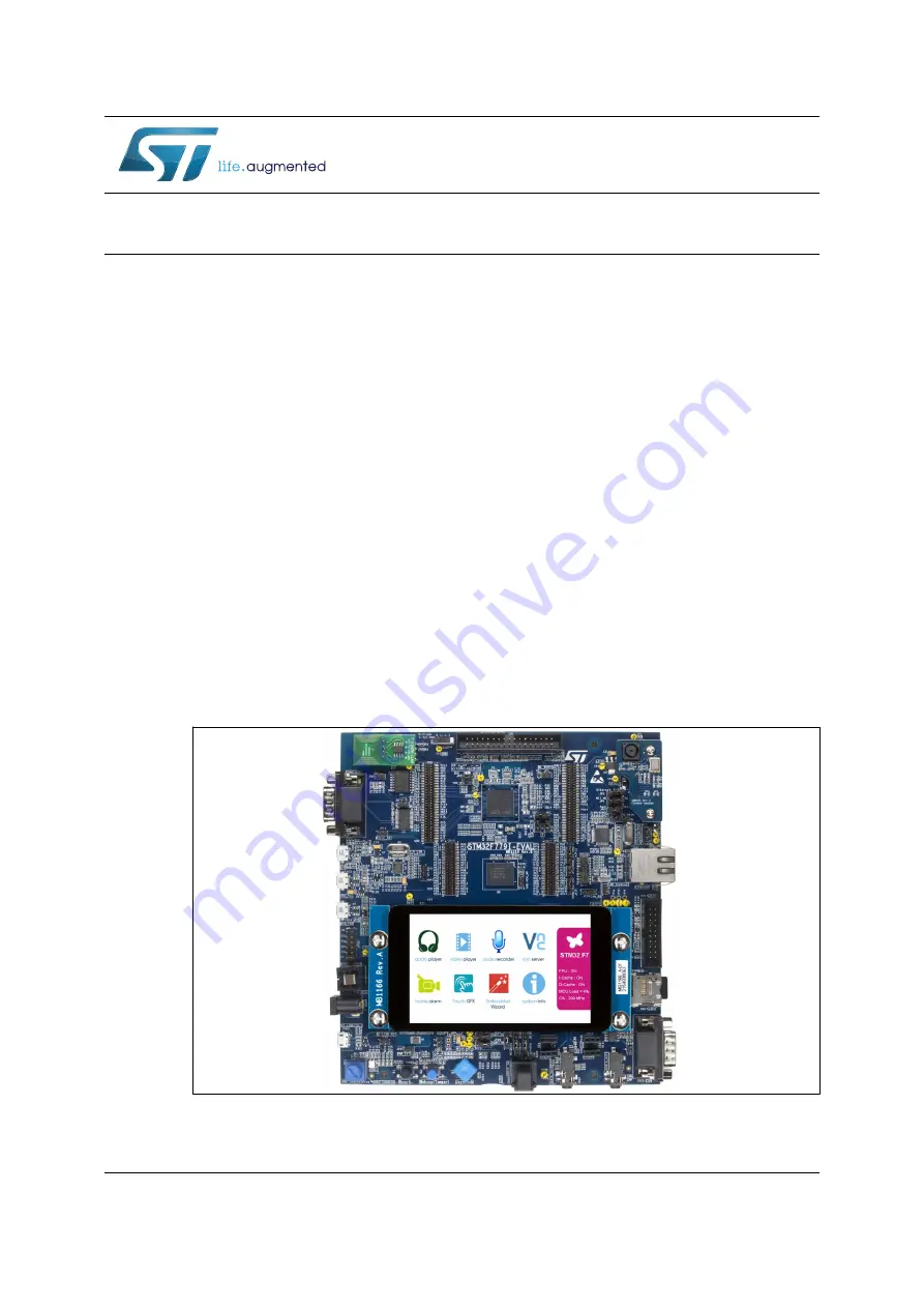
Figure 1. STM32F779I-EVAL evaluation board

1. Picture is not contractual.

www.st.com

Содержание STM32F779I-EVAL

Страница 1: ...d USB OTG FS peripherals SWD and JTAG debugging support Cryptographic acceleration hardware acceleration for AES 128 192 256 triple DES HASH MD5 SHA 1 SHA 2 and HMAC This evaluation board can be used as a reference design for user application development but it is not considered as a final application The full range of hardware features on the board helps the user to evaluate all the peripherals U...

Страница 2: ...6 1 1 Drivers 13 6 1 2 ST LINK V2 1 firmware upgrade 13 6 2 Power supply 14 6 3 Clock source 17 6 4 Reset source 18 6 5 Boot option 18 6 6 Audio 19 6 7 USB OTG1 FS 21 6 8 USB OTG2 HS and FS 21 6 9 RS 232 22 6 10 microSD cards 22 6 11 CAN 23 6 12 Ethernet 23 6 13 Memories 24 6 14 Quad SPI NOR Flash 25 6 15 Analog input 25 6 16 Camera module 26 6 17 Display and input devices 26 6 18 Motor control 27...

Страница 3: ... connector CN14 44 7 13 JTAG SWD connector CN16 44 7 14 microSD connectors CN17 and CN30 45 7 15 Power connector CN19 46 7 16 ST LINK V2 1 programming connector CN20 46 7 17 MFX programming connector CN21 46 7 18 ST LINK V2 1 USB Micro B connector CN22 46 7 19 MEMS microphone coupon connectors CN24 and CN25 47 7 20 CAN D type 9 pin male connector CN26 48 7 21 Audio jack speaker CN27 48 7 22 Audio ...

Страница 4: ...Contents UM2036 4 80 DocID029088 Rev 3 C 2 IC Compliance Statement 77 C 2 1 Compliance Statement 77 C 2 2 Déclaration de conformité 77 Appendix D CISPR32 78 D 1 Warning 78 Revision history 79 ...

Страница 5: ...ble 18 I2 C connector CN2 32 Table 19 Analog input output connector CN3 32 Table 20 Camera module connector CN4 33 Table 21 Daughterboard extension connector CN5 34 Table 22 Daughterboard extension connector CN6 36 Table 23 RS 232 connector CN7 38 Table 24 USB OTG HS Micro AB connector CN8 39 Table 25 RJ45 connector CN9 39 Table 26 Memory connector CN10 40 Table 27 Memory connector CN11 41 Table 2...

Страница 6: ...18 JTAG SWD debugging connector CN16 Top view 44 Figure 19 microSD connector Top view 45 Figure 20 Power supply connector CN19 Front view 46 Figure 21 USB Micro B connector Front view 47 Figure 22 MEMS microphone coupon connectors CN24 and CN25 Top view 47 Figure 23 CAN D type 9 pin male connector Front view 48 Figure 24 SPDIF IN connector CN29 Front view 49 Figure 25 STM32F779I EVAL evaluation bo...

Страница 7: ...nnector used to connect external speakers 4 Gbyte or more SDIO interface microSD card I2 C Extension interface RS 232 connector JTAG SWD and ETM trace debug support ST LINK V2 1 embedded IEEE 802 3 2002 compliant Ethernet connector Camera module 8Mx32bit SDRAM 1Mx16bit SRAM and 8Mx16bit NOR Flash 512 Mbit Quad SPI NOR Flash 4 capacitive touch LCD display with MIPI DSI connector Joystick with 4 dir...

Страница 8: ...y consequences deriving from such usage will not be at ST charge In no event ST will be liable for any customer usage of these engineering sample tools as reference design or in production E or ES marking examples of location On the targeted STM32 that is soldered on the board for illustration of STM32 marking refer to the section Package information of the STM32 datasheet at the www st com websit...

Страница 9: ...e board is extracted from its plastic bag check that no component remains in the bag The main components to verify are 1 25 MHz crystal X4 which may have been removed by a shock from its socket 2 The microSD card which may have been ejected from the connector CN17 right side of the board and CN30 bottom side Caution There is a risk of explosion if the battery is replaced by an incorrect one Accord...

Страница 10: ...to locate these features on the evaluation board The mechanical dimensions of the board are showed in Figure 4 The board history version is reported in the yellow frame of the Figure 25 Figure 2 Hardware block diagram 06Y 9 9 7 57 73 8 8 57 3 0 6 2 6 2 0 27 3 2 63 463 B 6 6 DQG 6 1 27 3 5 0 670 9 86 FRQQHFWRU H DNHXS 7DPSHU XWWRQV 3RWHQWLRPHWHU 1 FRQQHFWRU FRQQHFWRU FU VWDO 6 DQG WUDFH FRQQHFWRU 5...

Страница 11: ...4 FRORU LEDS CN26 CAN FRQQHFWRU CN17 PicroSD Fard1 CN24 CN25 Right Digital Microphone Coupon connectors CN27 Audio Line out FRQQHFWRU B2 Wakeup Eutton RV1 Potentiometer CN29 SPDIF_IN FRQQHFWRU CN15 DSI LCD FRQQHFWRU CN8 USB OTG2 HS CN13 USB OTG1 FS CN7 56 FRQQHFWRU CN14 USB OTG2 FS CN22 ST LINK V2 1 0LFUR 86 CN19 Power MDFN CN9 Ethernet B3 R stick CN16 JTAG DQG SWD CN2 I2 C H WHQVLRQ connector CN1...

Страница 12: ...e interface on USB USB power management request for more than 100 mA power on USB This feature is no more supported on the ST LINK V2 1 SWIM interface Minimum supported application voltage limited to 3 V 9 40 2 24 37 25 36 9 2 8 4 2 3 39 30 20 40 2 10 2 59 2 A 1 9 19 60 2 H 20 2 13 12 48 R 8 1 A 15 1 A 2 60 59 9 A 1 50 40 39 39 12 25 40 2 13 50 24 49 H 34 33 A 1 6 H R 16 17 24 25 15 28 8 7 12 13 2...

Страница 13: ...vers Before connecting the STM32F779I EVAL evaluation board to a Windows 7 Windows 8 or Windows XP PC via USB a driver for ST LINK V2 1 must be installed It can be downloaded from the www st com website In case the STM32F779I EVAL evaluation board is connected to the PC before installing the driver the PC device manager may report some STM32F779I EVAL interfaces as Unknown To recover from this sit...

Страница 14: ... be powered from ST LINK USB Micro B connector CN22 U5V but only the ST LINK circuit has the power before USB enumeration starting because the host PC only provides 100 mA to the boards at that time During the USB enumeration the STM32F779I EVAL board asks for the 300 mA power from the host PC If the host is able to provide the required power the target STM32 is powered and the red LED LD10 is tur...

Страница 15: ...o on to allow the board to be powered anyway but in any case the current will be limited to 600 mA by U17 ST890 The power supply is configured by setting the related jumpers JP2 JP15 and JP20 as described in Table 2 Table 2 Power supply related jumper settings Jumper Description JP2 JP2 is used to measure the STM32 current consumption manually by multimeter Default setting Fitted JP15 Vbat is conn...

Страница 16: ...1 FS CN13 when JP20 is set as shown on the right STM32F779I EVAL is supplied from the USB OTG2 HS CN8 when JP20 is set as shown to the right STM32F779I EVAL is supplied from power supply jack CN19 and daughterboard connected on CN5 and CN6 when JP20 is set as shown on the right daughterboard must not have its own power supply connected Table 2 Power supply related jumper settings continued Jumper ...

Страница 17: ...lock refers to Section 6 12 Ethernet Table 3 25 MHz crystal X1 related solder bridges Jumper Description SB40 PH0 is connected to 25 MHz crystal when SB40 is open Default setting PH0 is connected to extension connector CN5 when SB40 is closed In such case C23 X1 must be removed to avoid disturbance due to the 25 MHz quartz SB41 PH1 is connected to 25 MHz crystal when SB41 is open Default setting P...

Страница 18: ...witch SW1 BOOT and the boot base address programmed in the BOOT_ADD0 and BOOT_ADD1 option bytes The BOOT can be configured also via RS 232 connector CN7 Note R124 must be removed when boot loader starts up This prevents the USB_PHY continuous clock from interfering with the USART Rx IOs and the SPI Clock IOs Table 5 Boot related switch Switch configuration Boot address option bytes Boot space BOOT...

Страница 19: ...tion board They can be connected to either the audio codec or the DFSDM port of the STM32F779NI by setting jumpers shown in Table 7 Audio related jumpers The coupon connectors CN24 and CN25 can be used to support MEMS microphone evaluation board STEVAL MKI129V1 after removing SB78 and SB79 An optical connector CN29 is implemented on the STM32F779I EVAL to receive external audio data which is compa...

Страница 20: ...d to 3 3V power when JP22 is set as shown to the right Default setting Digital microphone power source is connected to MICBIAS1 from WM8994ECS R when JP22 is set as shown to the right JP3 PA2 is connected to SAI2_SCKB when JP3 is set as shown to the right Default setting PA2 is connected to MII_MDIO Ethernet when JP3 is set as shown to the right JP6 PC1 is connected to SAI1_SDA when JP6 is set as ...

Страница 21: ...ercurrent through the internal diode of the STM32F779NI 6 8 USB OTG2 HS and FS The STM32F779I EVAL evaluation board supports USB OTG2 High speed communication via a USB Micro AB connector CN8 USB high speed PHY U8 for high speed function Full speed communication via another USB Micro AB connector CN14 The evaluation board can be powered by these USB connectors CN8 or CN14 at 5 V DC with 500mA curr...

Страница 22: ... STM32F779NI are available on the board microSD card1 detection is managed by MFX GPIO15 and microSD card2 detection is managed by MFX GPIO10 Some PCB reworks are needed for microSD card1 application to disconnect peripherals which share I Os with microSD card1 and remove the camera module from the board Open SB17 SB72 Close SB75 SB76 Table 9 USART1 related jumpers Jumper Description JP21 USART1_R...

Страница 23: ...MII interface 25M clock can be generated by PHY or provided by MCO from STM32F779NI by setting jumper JP12 shown in Table 11 Ethernet related jumpers MII serial management signals MDIO and MDC are simulated by GPIOs PJ12 and PJ13 by default on the STM32F779I EVAL The original MII serial management signals of the Ethernet IP in the STM32F779NI can be also used by setting JP3 and JP6 Refer Table 7 A...

Страница 24: ... is set as shown to the right Default setting MDIO connect to MII_MDIO when JP4 is set as shown to the right JP8 MDC connect to MII_MDC when JP8 is set as shown to the right MDC connect to MII_MDC_GPIO when JP8 is set as shown to the right Default setting Table 12 Ethernet related solder bridges Solder bridges Description SB47 MII CRS on DP83848CVV is connected to PA0 when SB47 is closed and SB43 ...

Страница 25: ...ed A18 for 4 bit ETM to A21 for 1 bit ETM when the ETM trace is used In such cases memory addresses A19 to A22 not connected to FMC are pulled down so that memories can be addressed within a limited address range If A21 or A22 is required the camera board should be removed from the STM32F779I EVAL board 6 14 Quad SPI NOR Flash The 512 Mbit Quad SPI NOR Flash is connected to Quad SPI interface of t...

Страница 26: ... MIPI DSI interface of the STM32F779NI Users can connect MB1232 to DSI LCD connector CN15 to convert the DSI interface to the HDMI interface users can also connect MB1233 to CN15 to use RaspberryPI LCD Four general purpose color LEDs LD1 2 3 and 4 are available as display devices and they are connected respectively to PI15 PJ0 PJ1 and PJ3 of the STM32F779NI The 4 direction joystick B3 is connected...

Страница 27: ...Os to the motor control connector Solder bridges to be opened SB3 SB36 SB43 SB47 SB48 SB52 SB54 SB55 SB62 SB66 SB69 SB71 SB74 SB17 SB75 remove R93 R98 R245 R256 Keep no jumper on JP3 JP6 JP9 JP10 JP14 Keep CN4 and CN13 unconnected Solder bridges to be closed SB34 SB37 SB42 SB45 SB46 SB49 SB50 SB51 SB53 SB56 SB57 SB60 SB64 SB67 SB70 SB72 SB73 SB18 Mount R14 with 0 ohm resistor PA4 and PA5 are DAC o...

Страница 28: ... R51 R50 R49 TP6 U2 C5 R185 R183 R158 R157 R156 R154 R153 R151 TP19 TP18 TP15 TP14 TP12 R25 R225 CN28 D15 R186 R189 R184 R150 R145 R144 U13 R138 R139 U12 TP20 TP16 X4 JP8 X3 R6 R15 CN26 CN17 R142 R141 R143 CN16 R135 R134 R77 CN9 R73 R75 R74 C32 R71 C28 C31 C19 TP1 R128 R76 JP12 TP11 TP10 TP8 TP9 37 25 36 9 2 8 4 2 3 10 2 59 2 A 1 9 19 60 2 H 20 2 13 12 48 24 R 8 1 A 15 1 A 2 60 59 9 A 1 50 40 39 3...

Страница 29: ... R297 C177 R292 R295 C171 C105 R230 R226 SB35 C176 R263 SB65 SB61 SB63 SB59 SB44 C175 R294 R293 R296 C170 C110 C104 C178 C122 C125 C121 R258 R262 R260 SB58 C173 C172 C163 C157 C130 C127 C124 C120 C115 C113 R253 L7 R228 C162 R281 C119 R271 R270 R259 R261 R257 R255 C123 C109 C112 C114 C103 C147 C144 R278 R280 R279 C118 R269 R267 R268 C128 C108 SB40 SB41 R289 C148 R286 C137 R266 C135 C134 C107 SB39 C...

Страница 30: ... 15 PA5 MFX_GPIO5 Audio_INT Input Codec 16 PA6 MFX_GPIO6 OTG_FS1_ OverCurrent Input USB_FS1 17 PA7 MFX_GPIO7 OTG_FS1_ PowerSwitchOn Output USB_FS1 18 PB0 MFX_GPIO0 JOY_SEL Input Joystick 19 PB1 MFX_GPIO1 JOY_DOWN Input Joystick 20 PB2 MFX_GPIO2 JOY_LEFT Input Joystick 26 PB13 MFX_GPIO13 MII_INT Input Ethernet PHY 27 PB14 MFX_GPIO14 LCD_INT Input LCD 28 PB15 MFX_GPIO15 MicroSDcard Detect1 Input Mic...

Страница 31: ...ncy STOP PA6 1 2 GND MC_UH PC6 3 4 GND MC_UL PA7 5 6 GND MC_VH PC7 7 8 GND MC_VL PB0 9 10 GND MC_WH PC8 11 12 GND MC_WL PB1 13 14 PC4 BUS VOLTAGE CURRENT A PC1 15 16 GND CURRENT B PC2 17 18 GND CURRENT C PC3 19 20 GND NTC BYPASS RELAY PG11 21 22 GND DISSIPATIVE BRAKE PWM PH6 23 24 GND 5 V power 25 26 PC5 Heatsink temperature PFC SYNC PA12 and PA8 See Table 15 for details 27 28 3 3V power PFC PWM P...

Страница 32: ...CN3 Figure 10 Analog input output connector CN3 Top view Table 18 I2 C connector CN2 Pin number Description Pin number Description 1 I2C1_SDA PB9 5 3V3 2 NC 6 NC 3 I2C1_SCL PB8 7 GND 4 RESET PC10 8 NC 06 9 Table 19 Analog input output connector CN3 Pin number Description Pin number Description 1 analog input output PF10 2 GND 06Y 9 Ϯ ϭ ...

Страница 33: ... 1 8V 22 GND 3 GND 23 D0 PC6 4 GND 24 D1 PC7 5 D10 PD6 25 D2 PC8 6 D11 PD2 26 D3 PC9 7 GND 27 D4 PC11 8 GND 28 D5 PD3 9 D8 PC10 29 D6 PE5 10 D9 PC12 30 D7 PE6 11 GND 31 HSYNC PA4 12 GND 32 VSYNC PB7 13 I2C1_SCL PB8 33 PCLK PA6 14 I2C1_SDA PB9 34 Test point8 15 Camera_PLUG MFX GPIO12 35 Test point11 16 GND 36 Test point10 17 RST IN MFX GPIO11 37 GND 18 Test point 7 38 GND 19 XSDN MFX GPIO0 39 2 8V ...

Страница 34: ... 21 and Table 22 Table 21 Daughterboard extension connector CN5 Pin Description Alternative function How to disconnect with function block on STM32F779I EVAL board 1 GND 3 PH0 OSC_IN Remove X1 C23 Close SB40 5 RESET 7 PF6 QSPI_BK1_IO3 Remove R241 9 PF10 Potentiometer Remove R30 11 PC0 ULPI_STP Remove R123 13 PA2 SAI2_SCKB MII_MDIO MC_EnIndex Open SB37 SB35 15 PA0 SAI2_SDB MII_CRS MC_ENA Open SB43 ...

Страница 35: ...EmergencySTOP PAR_PCLK LCD_G2 Remove SB3 R14 22 PA7 MII_RX_DV MC_UL Open SB46 SB48 24 PA5 ULPI_CK Remove R124 26 PB1 ULPI_D2 MC_WL Open SB50 remove R98 28 PH4 ULPI_NXT Remove R121 30 GND 32 PI14 LCD_CLK 34 PJ4 LCD_R5 36 PB11 ULPI_D4 LCD_G5 Remove R104 open SB61 38 PB15 USB_FS2_DP Disconnect CN14 40 PH7 MII_RXD3 Remove R46 42 PJ5 LCD_R6 44 PJ6 46 PC5 MII_RXD1 MC_HEATSINK Open SB67 SB69 48 3V3 50 GN...

Страница 36: ...D_HSYNC 9 PI8 EXPANDER_INT Remove R296 11 PK6 LCD_B7 13 PK4 LCD_B5 15 PG12 SPDIF_RX1 Remove R206 17 PG9 SAI2_FSB SD2_D0 LRCLK Remove R172 disconnect DSI and SD2 19 GND 21 PB7 LED3 PAR_ VSYNC Disconnect CN4 23 PD3 DFSDM_CLK JP24 open 25 PG13 MII_TXD0 Remove R248 27 PJ12 LCD_B0 29 PG14 MII_TXD1 Remove R249 31 PB8 I2C1_SCL Remove R175 R5 R293 disconnect CN4 CN15 and CN18 33 PG11 MII_TX_EN MC_NTC Open...

Страница 37: ...N15 and CN18 16 PK3 LCD_B4 18 PB6 QSPI_BK1_NCS Remove R230 20 PJ14 LCD_B2 22 PJ15 LCD_B3 24 PB4 JTRST SD2_D3 Open SB16 disconnect SD2 26 PJ13 LCD_B1 28 PC12 SD1_CK PAR_D9 Disconnect CN4 disconnect SD1 30 GND 32 PA15 JTDI Remove R99 34 PK1 36 PA14 JTCK SWCLK Remove R91 38 PK2 40 PA13 JTMS SWDIO Remove R84 42 PA12 CAN1_TX USB_FS1_DP MC_PFCsync2 Open SB60 SB62 SB66 44 PA10 RS232_RX USB_FS1_ID Remove ...

Страница 38: ...isconnect SD2 58 PC6 MC_UH PAR_D0 I2S3_CK Open SB18 disconnect CN4 keep JP9 on open 60 5 V Table 22 Daughterboard extension connector CN6 continued Pin Description Alternative Function How to disconnect with function block on STM32F779I EVAL board Table 23 RS 232 connector CN7 Pin number Description Pin number Description 1 NC 6 Bootloader_BOOT 2 RS232_RX PA10 7 NC 3 RS232_TX PA9 8 Bootloader_RESE...

Страница 39: ...on these two connectors The space between these two connectors is defined as a standard which allows to develop common daughterboard The standard width between CN10 pin 1 and CN11 pin 1 is 1914 mils 48 62 mm For more details on signal assignment refer to Table 27 and Table 28 Table 24 USB OTG HS Micro AB connector CN8 Pin number Description Pin number Description 1 VBUS 4 ID 2 D 5 GND 3 D Table 25...

Страница 40: ...I_COL Open SB57 3 PF13 A7 5 PF12 A6 7 PG1 A11 9 GND 11 PE7 D4 13 PE10 D7 15 PE12 D9 17 PE15 D12 19 PE13 D10 21 PD11 A16 23 PD12 A17 25 PG5 A15 BA1 27 PH11 D19 29 GND 31 PD13 A18 33 PG2 A12 35 PD8 D13 37 PD9 D14 39 PD14 D0 2 PH5 SDNWE 4 PF14 A8 6 PG0 A10 8 PF11 SDNRAS 10 GND 12 PE9 D6 14 PE8 D5 16 PE11 D8 18 PF15 A9 20 PE14 D11 22 PH8 D16 24 PH10 D18 26 PH9 D17 28 PG4 A14 BA0 ...

Страница 41: ...G7 GND NAND_INT Short pin 2 3 of JP13 when connect NAND module to CN11 close SB19 in any other case short pin 1 and 2 of JP13 11 PE4 A20 TRACED1 Open SB11 13 PE3 A19 TRACED0 Open SB9 15 PI5 NBL3 17 PI4 NBL2 19 PG15 SDNCAS 21 PI10 D31 MII_RX_ER Open SB12 23 PE1 NBL1 25 PE0 NBL0 27 PG6 NE3 LCD_R7 Close SB20 29 GND 31 PD0 D2 33 PI2 D26 35 PI1 D25 37 PI0 D24 39 PH13 D21 2 PH2 SDCKE0 4 PE5 A21 TRACED2 ...

Страница 42: ... PI7 D29 20 PI9 D30 22 PI6 D28 24 PC7 NE1 MC_VH PAR_D0 Connect JP10 disconnect CN4 CN1 26 PD5 NWE 28 PD4 NOE 30 GND PC8 GND NAND_NCE PAR_D0 Short pin 2 3 of JP17 open SB72 SB75 close SB18 disconnect CN4 CN1 when connect NAND module to CN11 in any other case short pin 1 2 of JP17 32 PD1 D3 34 PI3 D27 36 PH15 D23 38 PH14 D22 40 3 3V Table 27 Memory connector CN11 continued Pin Description Alternativ...

Страница 43: ...umber Description Pin number Description 1 3 3V 2 TMS PA13 3 GND 4 TCK PA14 5 GND 6 TDO PB3 7 KEY 8 TDI PA15 9 GND 10 RESET 11 GND 12 TraceCLK PE2 13 GND 14 TraceD0 PE3 or SWO PB3 15 GND 16 TraceD1 PE4 or nTRST PB4 17 GND 18 TraceD2 PE5 19 GND 20 TraceD3 PE6 Table 29 USB OTG1 FS Micro AB connector CN13 Pin number Description Pin number Description 1 VBUS PA9 4 ID PA10 2 D PA11 5 GND 3 D PA12 ...

Страница 44: ...or CN16 Figure 18 JTAG SWD debugging connector CN16 Top view Table 30 USB OTG2 FS Micro AB connector CN14 Pin number Description Pin number Description 1 VBUS PB13 4 ID PB12 2 D PB14 5 GND 3 D PB15 Table 31 JTAG SWD debugging connector CN16 Pin number Description Pin number Description 1 3 3V 2 3 3V 3 PB4 4 GND 5 PA15 6 GND 7 PA13 8 GND 9 PA14 10 GND D ϯϬϳϮϮsϮ ...

Страница 45: ...17 DBGRQ 18 GND 19 DBGACK 20 GND Table 31 JTAG SWD debugging connector CN16 continued Pin number Description Pin number Description Table 32 microSD card1 connector CN17 Pin number Description Pin number Description 1 SDMMC_D2 PC10 6 Vss GND 2 SDMMC_D3 PC11 7 SDMMC_D0 PC8 3 SDMMC_CMD PD2 8 SDMMC_D1 PC9 4 3 3V 9 GND 5 SDMMC_CLK PC12 10 MicroSDcard_detect1 MFX GPIO15 ...

Страница 46: ...ing It is not populated by default and not for end user 7 17 MFX programming connector CN21 The connector CN21 is used only for MFX Multi Function expander programming during the board manufacturing It is not populated by default and not for end user 7 18 ST LINK V2 1 USB Micro B connector CN22 The USB connector CN22 is used to connect the embedded ST LINK V2 1 to the PC to debug the board Table 3...

Страница 47: ...Figure 22 MEMS microphone coupon connectors CN24 and CN25 Top view Table 34 USB Micro B connector CN22 Pin number Description Pin number Description 1 VBUS power 4 ID 2 DM 5 GND 3 DP 6 7 8 9 10 11 Shield Table 35 MEMS microphone coupon connectors CN24 and CN25 Pin number Description Pin number Description 1 DATA 4 VDD 2 GND 5 L R 3 CLK 6 NC ...

Страница 48: ... CN27 for speaker out is available on the STM32F779I EVAL evaluation board to support external speaker 7 22 Audio jack CN28 A 3 5mm stereo audio jack CN28 is available on the STM32F779I EVAL evaluation board to support headset headphone and microphone integrated Table 36 CAN D type 9 pin male connector CN26 Pin number Description Pin number Description 1 4 8 9 NC 7 CANH 2 CANL 3 5 6 GND 3 6 ...

Страница 49: ...Rev 3 49 80 UM2036 Connectors 79 7 23 SPDIF IN connector CN29 Figure 24 SPDIF IN connector CN29 Front view Table 37 SPDIF IN connector CN29 Pin number Description Pin number Description 1 SPDIF_RX1 PG12 3 VCC 2 GND ...

Страница 50: ...ACP and RF_I2C1_SCL A8 PB5 ULPI_D7 LCD_G7 A9 PB4 NJTRST SD2_D3 A10 PB3 JTDO SD2_D2 A11 PD7 SD2_CMD A12 PC12 SD1_CK D9 A13 PA15 JTDI A14 PA14 JTCK SWCLK A15 PA13 JTMS SWDIO B1 PE5 A21 TRACED2 LCD_G0 D6 B2 PE6 A22 SAI2_MCLK_B TRACED3 LC D_G1 D7 B3 PG13 MII_TXD0 B4 PB9 Audio and EXPANDER and ACP and RF_I2C1_SDA B5 PB7 VSYNC B6 PB6 QSPI_BK1_NCS CEC B7 PG15 SDNCAS B8 PG11 MII_TX_EN NTC_BYPASS_IO B9 PJ1...

Страница 51: ...7 C14 PI2 D26 C15 PA11 CAN1_RX USB_FS1_DM PFC_PWM_TIM1_1_CH4 D1 PC13 ANTI_TAMP KEY_ TAMP1_WKUP2 D2 PF0 A0 D3 PI5 NBL3 D4 PI7 D29 D5 PI10 D31 MII_RX_ER D6 PI6 D28 D7 PK4 LCD_B5 D8 PK3 LCD_B4 D9 PG9 SAI2_FS_B SD2_D0 D10 PJ15 LCD_B3 D11 PD4 NOE D12 PD2 SD1_CMD D11 D13 PH15 D23 D14 PI1 D25 D15 PA10 RS232_USART1_RX USB_FS1_I D E1 PC14 OSC32_IN OSC32_IN Table 38 STM32F779I EVAL I O assignment continued ...

Страница 52: ...2_USART1_TX USB_FS1_VBUS F1 PC15 OSC32_OUT OSC32_OUT F2 VSS_18 F2 VSS_13 F3 PI11 ULPI_DIR LCD_G6 F4 VDD_13 F5 VDD_17 F6 VSS_3 F7 VSS_11 F8 VSS_10 F9 VSS_15 F10 VSS 2 F11 VDD_2 F12 PK1 F13 PK2 F14 PC9 SD1_D1 LCD_G3 D3 F15 PA8 Backlight_PWM_TIM1_CH1 MII_MCO PFC_SYNC1_TIM1_1_CH1 G1 PH0 OSC_IN OSC_IN Table 38 STM32F779I EVAL I O assignment continued Pin No Pin Name STM32F779I EVAL standard Motor contr...

Страница 53: ...IM8_CH2 D1 H1 PH1 OSC_OUT OSC_OUT H2 PF3 A3 H3 PI14 LCD_CLK H4 PH4 ULPI_NXT H5 VDD_5 H6 VSS_5 H10 VSS_20 H11 VDD_20 H12 PJ8 H13 PJ10 H14 PG8 SDCLK MII_PPS_OUT H15 PC6 FMC_NWAIT UH_TIM8_CH1 D0 J1 NRST NRST J2 PF4 A4 J3 PH5 SDNWE J4 PH3 SDNE0 MII_COL J5 VDD_12 J6 VSS_12 J10 VSS_8 J11 VDD_8 J12 PJ7 J13 PJ9 Table 38 STM32F779I EVAL I O assignment continued Pin No Pin Name STM32F779I EVAL standard Moto...

Страница 54: ...J6 K13 PD15 D1 K14 PB13 ULPI_D6 USB_FS2_VBUS K15 PD10 D15 L1 PF10 POT_ADC3_IN8 L2 PF9 QSPI_BK1_IO1 L3 PF8 QSPI_BK1_IO0 L4 PC3 MII_TX_CLK CURRENT_C_ADC3_123_IN13 L5 BYPASS_RE G L6 VSS_19 L7 VDD_19 L8 VDD_6 L9 VDD_7 L10 VDD_1 L11 VCAP1 L12 PD14 D0 L13 PB12 ULPI_D5 USB_FS2_ID L14 PD9 D14 L15 PD8 D13 M1 VSSA Table 38 STM32F779I EVAL I O assignment continued Pin No Pin Name STM32F779I EVAL standard Mot...

Страница 55: ...ENCODER_B_TIM5_5_CH2 N3 PA0 WKUP SAI2_SD_B MII_CRS ENCODER_A_TIM5_5_CH1 N4 PA4 DAC_OUT1 HSYNC N5 PC4 MII_RXD0 BUSVOLTAGE_ADC12_IN14 N6 PF13 A7 N7 PG0 A10 N8 PJ3 LCD_R4 LED3 N9 PE8 D5 N10 PD11 A16 N11 PG5 A15 BA1 N12 PG4 A14 BA0 N13 PH7 MII_RXD3 N14 PH9 D17 N15 PH11 D19 P1 VREF P2 PA2 SAI2_SCK_B MII_MDIO INDEX_TIM5_5_CH3 P3 PA6 STOP_TIM8_BKIN PIXCLK P4 PA5 ULPI_CK DAC_OUT2 P5 PC5 MII_RXD1 HEATSINK_...

Страница 56: ...4 PH8 D16 P15 PH10 D18 R1 VDDA R2 PA3 ULPI_D0 R3 PA7 MII_RX_DV UL_TIM8_CH1N R4 PB1 ULPI_D2 WL_TIM8_CH3N R5 PB0 ULPI_D1 VL_TIM8_CH2N R6 PJ0 LCD_R1 LED1 R7 PJ1 LCD_R2 LED2 R8 PE7 D4 R9 PE10 D7 R10 PE12 D9 R11 PE15 D12 R12 PE13 D10 R13 PB11 ULPI_D4 R14 PB14 USB_FS2_DM R15 PB15 USB_FS2_DP Table 38 STM32F779I EVAL I O assignment continued Pin No Pin Name STM32F779I EVAL standard Motor control variant C...

Страница 57: ...er supply see Figure 27 SRAM Flash SDRAM see Figure 28 Audio amplifier see Figure 29 LCD camera and connector see Figure 30 Ethernet see Figure 31 USB OTG HS see Figure 32 USB OTG FS see Figure 33 RS 232 see Figure 34 CAN and Quad SPI see Figure 35 Peripherals see Figure 36 Motor control Figure 37 Extension connectors see Figure 38 ST LINK V2 1 see Figure 39 MFX and LEDs see Figure 40 SWD and JTAG...

Страница 58: ...FS1_ID U_USB_OTG_FS USB_OTG_FS SchDoc 25MHz clock 24MHz clock 3 2 1 JP26 Same length RS232_TX RS232_RX Bootloader_BOOT0 Bootloader_RESET U_RS232 RS232 SchDoc 3 2 1 JP21 LCD_R 0 7 LCD_HSYNC LCD_VSYNC LCD_CLK LCD_ENB LCD_BL_CTRL I2C1_SDA I2C1_SCL LCD_B 0 7 LCD_G 0 7 RSTI XSDN PAR_HSYNC PAR_PCLK PAR_VSYNC PAR_D 0 11 EXT_RESET LCD_INT Camera_PLUG RESET DSI SCLK MCLK LRCLK SPDIF I2S CEC_CLK CEC U_LCD C...

Страница 59: ... R26 33 R43 33 R44 33 X2 NX3215SA 32 768KHZ EXS00A MU00525 SB45 Open SB43 Closed SB34 Open SB36 Closed SB37 Open SB3 Closed SB46 Open SB48 Closed SB71 Closed SB62 Closed SB66 Closed SB70 Open SB74 Open SB64 Open SB60 Open SB73 Open SB50 Open SB65 Open SB76 Closed SB10 Closed SB11 Closed SB9 Closed SB7 Closed SB6 Closed SB25 Closed SB26 Closed SB27 Closed SB57 Open SB20 Closed SB19 Closed SB53 Open...

Страница 60: ...C53 47uF C55 10uF C56 100nF 5V 3V3 TP13 Ground TP4 3V3 1 3 2 CN19 DC 10B Z1 SMAJ5 0A TR C62 100nF 1 2 3 D13 ZEN056V130A24LS E5V D5V U5V_ST_LINK 5V C19 10uF 2V8 TP3 2V8 R15 120 C5 10uF R6 150 C61 10uF 1V8 TP6 1V8 3V3 3V3 VDD_MCU JP2 R140 820 VBUS_HS VBUS_FS1 1 2 3 4 5 6 7 8 9 10 11 12 JP20 Header 6X2 VBUS_FS2 TP1 Ground TP2 Ground TP26 Ground Vin 3 Vout 2 Tab 4 GND 1 U18 LD1086D2M33 Vin 3 Vout 2 Ta...

Страница 61: ... G9 A0 G8 NC E3 DQ0 R8 DQ8 L2 DQ1 N7 DQ9 M3 DQ2 R9 DQ10 M2 DQ3 N8 DQ11 P1 VDDQ B2 DQ4 P9 DQ12 N2 DQ5 M8 DQ13 R1 DQ6 M7 DQ14 N3 DQ7 L8 DQ15 R2 VSS A3 VDD A7 DQ16 E8 DQ24 A2 DQ17 D7 DQ25 C3 DQ18 D8 DQ26 A1 DQ19 B9 DQ27 C2 DQ20 C8 DQ28 B1 DQ21 A9 DQ29 D2 DQ22 C7 DQ30 D3 DQ23 A8 DQ31 E2 VSSQ B3 VDDQ B7 VSSQ B8 VSSQ C1 VDDQ C9 VSSQ D1 VDDQ D9 VDDQ E1 NC E7 VSSQ E9 VSS F1 VDD F9 NC H3 NC H7 BA0 J7 BA1 H...

Страница 62: ...LP A2 SPKOUTRN C3 SPKOUTRP B3 SPKVDD1 B2 SPKVDD2 C2 VMIDC C9 VREFC E6 U20 WM8994ECS R C77 100nF C68 100nF 3V3 1V8 3V3 SAI2_FSB SAI2_SDB SAI1_SDA PA2 PG9 PC1 Audio_INT C64 1uF I2C1_SDA I2C1_SCL PB9 PB8 SAI2_MCLKB PE6 R164 2K2 C75 100nF C76 100nF R165 20 R166 20 C72 2 2uF C70 2 2uF C74 2 2uF 3 2 1 JP22 3 2 1 JP23 3 2 1 JP24 MICBIAS1 3V3 C87 100nF DFSDM_CLK time slot1 of SAI time slot0 of SAI DFSDM_D...

Страница 63: ...SET R162 0 To MFX MFX_GPIO12 MFX_GPIO14 R233 10K PD2 PD6 PC12 3V3 To MFX I2C1_SDA_C R236 N A R239 N A From MFX TP10 TP9 TP8 TP11 MFX_GPIO11 1V8 1V8 LCD_G 0 7 LCD_R 0 7 LCD_B 0 7 PAR_D 0 11 1 2 3 4 5 6 7 8 9 10 11 12 13 14 15 16 17 18 19 20 21 22 23 24 25 26 27 28 29 30 31 32 33 34 35 36 37 38 39 40 42 41 CN4 F1000 2 20MGF L0A FTSH 125 01 F DV K Samtec SSM 104 L DH Samtec CLM 120 02 L D Samtec H4 H...

Страница 64: ... AN_EN 26 LED_SPEED AN1 27 LED_LINK AN0 28 RESET_N 29 MDIO 30 MDC 31 IOVDD33 32 X2 33 X1 34 IOGND 35 DGND 36 PFBIN2 37 RX_CLK 38 RX_DV MII_MODE 39 CRS CRS_DV LED_CFG 40 RX_ER MDIX_EN 41 COL PHYAD0 42 RXD_0 PHYAD1 43 RXD_1 PHYAD2 44 RXD_2 PHYAD3 45 RXD_3 PHYAD4 46 IOGND 47 IOVDD33 48 U6 DP83848CVV 3V3 C27 100nF C32 100nF C36 100nF R73 1K5 TP12 25MHz TD 1 TCT 4 TD 2 RD 3 RCT 5 RD 6 NC 7 CHS GND 8 LE...

Страница 65: ...0 7 PB11 PB12 PB13 PB5 ULPI_D4 ULPI_D5 ULPI_D6 ULPI_D7 L2 EXC 3BP121H BEAD L1 EXC 3BP121H BEAD R92 10K R101 820 R94 330 1 2 LD5 Green R82 47K R78 22K C42 100nF C33 100nF C43 100nF C34 100nF RESET PH4 PI11 PC0 PA5 3 1 2 T6 9013 3V3 A1 A2 B1 B2 D4 USBULC6 2F3 A1 A2 B1 B2 D3 ESDA14V2 2BF3 3V3 3V3 GND 2 IN 5 EN 4 OUT 1 FAULT 3 U7 STMPS2151STR USB_FS2_DM USB_FS2_DP VBUS 1 DM 2 DP 3 ID 4 GND 5 Shield 6 ...

Страница 66: ...rrent 3V3 1 2 LD8 Red R127 620 USB_FS1_DM USB_FS1_DP USB_FS1_ID C47 4 7uF R130 0 R115 0 R132 0 GND 2 IN 5 EN 4 OUT 1 FAULT 3 U11 STMPS2151STR VBUS 1 DM 2 DP 3 ID 4 GND 5 Shield 6 USB_Micro AB receptacle Shield 7 Shield 8 Shield 9 EXP 10 CN13 475900001 VBUS_FS1 PA9 PA10 PA11 PA12 R116 330 1 2 LD7 Green 3V3 R103 22K From MFX To MFX MFX_GPIO6 MFX_GPIO7 R129 10K R131 47K R106 47K 3 1 2 T7 9013 D2_N D2...

Страница 67: ...RX 3V3 3V3 Bootloader_BOOT0 Bootloader_RESET PA9 PA10 RXD TXD CTS DSR RS232 C133 100nF C25 100nF C132 100nF C131 100nF C26 100nF C2 1 C2 2 V 3 R1IN 4 R2IN 5 R3IN 6 R4IN 7 R5IN 8 T1OUT 9 T2OUT 10 T3OUT 11 T3IN 12 T2IN 13 T1IN 14 R5OUT 15 R4OUT 16 R3OUT 17 R2OUT 18 R1OUT 19 R2OUTB 20 R1OUTB 21 nSHDN 22 nEN 23 C1 24 GND 25 VCC 26 V 27 C1 28 U5 ST3241EBPR 1 6 2 7 3 8 4 9 5 CN7 DB9 male USART1 JP11 ...

Страница 68: ...189 0 R186 0 R184 N A Default setting 1 2 Default setting Open PA12 PA11 CAN C179 100nF R183 10K 3 1 2 D15 ESDCAN24 2BLY Optional Quad SPI Flash QSPI_BK1_IO0 QSPI_BK1_IO3 QSPI_BK1_IO2 QSPI_BK1_IO1 PF8 PF9 PF7 PF6 QSPI_CLK PB2 QSPI_BK1_NCS R230 10K PB6 C105 100nF MICRON 3V3 3V3 N25Q512A13GSF40E MICRON CS 7 DQ1 8 NC 6 NC 5 NC 12 NC 11 Vss 10 W Vpp DQ2 9 HOLD DQ3 1 VCC 2 NC 3 CLK 16 DQ0 15 NC 4 NC 13...

Страница 69: ... CN3 two pin header for external analog input R28 47 C97 100nF R30 0 3V3 To MFX 3V3 MICRO SD2 3V3 SMS064FF or SMS128FF 1 2 3 4 5 6 7 8 SW2 9 SW1 10 CN30 PJS008 2000 R224 0 3V3 TF Card To MFX input with pull up MFX_GPIO10 R205 47K R202 47K R201 47K R204 47K R203 47K 3V3 R200 10K N A Potentiometer Joystick MFX_GPIO0 MFX_GPIO1 MFX_GPIO2 MFX_GPIO3 MFX_GPIO4 MICRO SD1 3V3 SMS064FF or SMS128FF 1 2 3 4 5...

Страница 70: ... SYNC 27 PFC PWM 29 Encoder A 31 Encoder B 33 GND 2 GND 4 GND 6 GND 8 GND 10 GND 12 BUS VOLTAGE 14 GND 16 GND 18 GND 20 GND 22 GND 24 Heatsink Temperature 26 Vdd_Micro 28 GND 30 GND 32 Encoder Index 34 CN1 MC_connector MC_EmergencySTOP MC_CurrentA MC_CurrentB MC_CurrentC MC_PFCsync1 MC_PFCsync2 MC_WL MC_VH MC_VL MC_UH MC_UL MC_WH MC_NTC MC_DissipativeBrake MC_PFCpwm MC_EnA MC_EnB MC_Heatsink MC_Bu...

Страница 71: ...PH12 PH3 PH5 Place close Memory D13 D14 D15 A16 A17 A18 D0 D1 D4 D5 D6 D7 D8 D9 D10 D11 D12 SDNRAS A6 A7 A8 A9 A11 A12 A13 A14 A15 SDCLK SDNE0 SDNWE D16 D17 D18 D19 D20 Left Right 1 2 3 4 5 6 7 8 9 10 11 12 13 14 15 16 17 18 19 20 21 22 23 24 25 26 27 28 29 30 31 32 33 34 35 36 37 38 39 40 41 42 43 44 45 46 47 48 49 50 51 52 53 54 55 56 57 58 59 60 CN5 P1039 2 30MGF 089 1A 1 2 3 4 5 6 7 8 9 10 11 ...

Страница 72: ..._1 23 PA4 14 PB3 JTDO 39 PA5 15 VDD_1 24 PA6 16 PB4 JNTRST 40 PB12 25 PB5 41 PB13 26 PB6 42 PB14 27 PB7 43 PB15 28 BOOT0 44 PA8 29 PB8 45 PA9 30 PB9 46 PA10 31 VSS_3 47 PA11 32 VDD_3 48 U21 STM32F103CBT6 R295 100K D12 BAT60JFILM Power Switch to supply 5V from STLINK USB PWR_ENn 3V3_ST_LINK 1 2 3 4 5 CN20 N A C169 100nF C171 100nF C176 100nF C174 100nF 3V3_ST_LINK 3V3_ST_LINK JP25 N A R292 N A Not ...

Страница 73: ... R215 680 R213 680 LEDs 3V3 3V3 3V3 3V3 Default I2C Address 1000010 3V3 R171 N A MFX_V3 WAKEUP 2 NRST 7 TSC_XP GPO0 10 TSC_XN GPO1 11 TSC_YP GPO2 12 TSC_YN GPO3 13 USART_TX 21 USART_RX 22 SPARE 14 SWDIO 34 SWCLK 37 I2C_SCL 42 I2C_SDA 43 BOOT0 44 I2C_ADDR 45 IRQOUT 46 IDD_CAL GPO4 3 IDD_SH0 4 IDD_SH1 GPO5 5 IDD_SH2 GPO6 6 IDD_MEAS 25 GPIO0 18 GPIO1 19 GPIO2 20 GPIO3 39 GPIO4 40 GPIO5 15 GPIO6 16 GP...

Страница 74: ...A R138 N A R141 N A R134 N A R142 N A 1 2 3 4 5 6 7 8 9 10 11 12 13 14 15 16 17 18 19 20 CN16 JTAG R144 10K R145 10K R143 10K R109 N A R111 N A TDI RESET TRACE_D3 TRACE_D2 TRACE_D1 TRACE_D0 TRACE_CK TRST TMS SWDIO TCK SWCLK TDO SWO Trace connector JTAG connector KEY PA13 PA14 PB3 PA15 PB4 PE6 PE5 PE4 PE3 PE2 R135 N A 3V3 3V3 3V3 3V3 R84 22 R91 22 R97 22 R99 22 R110 22 R102 22 FTSH 110 01 L DV Samt...

Страница 75: ...connector for LCD panel HSSI_CLK_N HSSI_CLK_P HSSI_D0_N HSSI_D0_P HSSI_D1_N HSSI_D1_P TE C9 100nF VDD RST RST CABC CABC R1 0 INT R6 N A R7 N A VDD R8 4K7 I2C_SDA I2C_SCL HSSI_CLK_N HSSI_CLK_P HSSI_D0_N HSSI_D0_P HSSI_D1_N HSSI_D1_P TE RST C8 100nF HSSI_CLK_N 12 NC 13 HSSI_CLK_P 14 GND 15 HSSI_D1_N 16 NC 17 HSSI_D1_P 18 GND 19 NC ERR 20 VCC 21 TE 22 LEDK 23 LEDA 24 GND 25 IOVCC 6 ID 1 GND 2 CABC 3 ...

Страница 76: ... R5 0 D1 BAT60JFILM supply voltage 2 5V 10 BAT60 VF 0 28 10mA 0 35 100mA default system clock using clock from mother board C4 100nF AGND 1 NC 16 AVDD 2 8V 4 SDA 20 RESET 22 VSYNC 23 PWDN 24 HSYNC 25 DVDD 1 8V 6 DOVDD 2 8V 8 D7 7 MCLK 12 D6 9 DGND 27 D5 11 PCLK 29 D4 13 D8 5 D3 15 D9 3 D2 17 SCL 18 NC 10 NC 30 NC 28 D1 19 D0 21 NC 2 FLASH 14 SHUTTER 26 CN1 AXE530124 PAR_D 0 7 Camera_CLK R8 N A SCL...

Страница 77: ...easonable protection against harmful interference when the equipment is operated in a commercial environment This equipment generates uses and can radiate radio frequency energy and if not installed and used in accordance with the instruction manual may cause harmful interference to radio communications Operation of this equipment in a residential area is likely to cause harmful interference in wh...

Страница 78: ...CISPR32 UM2036 78 80 DocID029088 Rev 3 Appendix D CISPR32 D 1 Warning Warning This device is compliant with Class A of CISPR32 In a residential environment this equipment may cause radio interference ...

Страница 79: ...ion Changes 23 May 2016 1 Initial release 02 Dec 2016 2 Added sections Section Appendix C Federal Communications Commission FCC and Industry Canada IC Compliance Statements Section Appendix D CISPR32 08 Mar 2017 3 Added boot loader note in Section 6 5 Boot option and ESD protection note in Section 6 7 USB OTG1 FS ...

Страница 80: ...asers are solely responsible for the choice selection and use of ST products and ST assumes no liability for application assistance or the design of Purchasers products No license express or implied to any intellectual property right is granted by ST herein Resale of ST products with provisions different from the information set forth herein shall void any warranty granted by ST for such product S...

Отзывы: