XAV-AX150
XAV-AX150
36
Sony CONFIDENTIAL
For Authorized Servicer
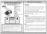
5-6. SCHEMATIC DIAGRAM - MAIN Board (1/4) -
• See page 45 for Waveforms. • See page 46 for IC Block Diagrams. • See page 51 for IC Pin Function Description.
1
3.2
1.7
1.6
1.6
0
1.6
1.6
0
3.3
1.6
1.6
1.6
1.5
1.6
1.6
1.6
1.5
1.6
3.3
3.3
3.3
0
3.3
0
3.2
0
3.3
0.6
2.4
0
0
3.3
1.6
1.5
1.6
3.3
3.3
0
0
0
0
3.3
1.2
0
3.3
0.5
2.3
2.6
1.3
4
4
1.5
1.6
1.6
1.6
0
0
0
1.7
3.3
1.2
0
3.3
3.3
1.3
1.3
3.3
4.7
C726
10
C730
10
C744
C608
47
C601
1
C600
10
1
C609
1
C607
1
C605
2.2
C619
60P
CN201
USB1_VBUS 5V
1
USB1_VBUS 5V
2
USB1_VBUS 5V
3
USB1_GND
4
USB1_GND
5
USB1_GND
6
SOC 4V
7
SOC 4V
8
SOC 4V
9
SOC 4V
10
SOC 4V
11
SOC_GND
12
SOC_GND
13
SOC_GND
14
SOC_GND
15
SOC_GND
16
SOC_GND
17
LCD 5V
18
19
FB_5V(SOC_GND)
L_GND
20
LCD_RST
21
AUX_L
22
AUX_GND
23
AUX_R
24
RE0
25
RE1
26
USB_D+
27
KEY
A/D
28
USB_D–
29
LED PWM
30
VBUS_GND
31
SIRCS
32
KEY_GND
33
KEY_GND
34
Maestro_TX
35
Maestro_RX
36
SOC UAR
T
RX
37
SOC UAR
T
TX
38
VIDEO I2C SCL
39
VIDEO I2C SDA
40
D_GND
41
Reset
42
CDP/SDP
43
USB F
AUL
T
44
USB EN
45
D_GND
46
USB_SEL
47
REVERSE_CTL
48
VDO_RST
49
VDO_MUTE
50
GUIDANCE
51
CAMERA
CVBS GND
52
CAMERA
CVBS
53
A_GND
54
AUDIO R
55
AUDIO GND
56
AUDIO L
57
A_GND
58
MIC AUDIO
59
MIC GND
60
1SS387-TPL3
D601
DZ2J06800L
D600
FB600
FB700
J600
JL613
JL610
JL606
JL608
JL601
JL612
JL602
JL607
JL605
JL604
JL615
JL61
1
JL603
JL609
IC700
LC786823E-6E21-3H
1
NC
2
A
VDD1
3
A
VSS1
4
LRREF
5
DACOUTR
6
RV
R
IN
7
RROUT
8
RFOUT
9
DACOUTS
10
SWIN
11
SWOUT
12
VREF_ADC
13
A
VSS2
14
A
VDD2
15
L3INP
16
L3INN
17
R3INP
18
R3INN
19
L2IN
20
R2IN
21
L1IN(BT_MIC)
22
R1IN(BT_MIC)
23
TEST0
24
TEST1
25
DVDD18_2
26
BT_RST
27
CD_DI
28
CD_CL
29
CD_DO
30
CD_CE
31
DVDD
32
DVSS
33
BT_DOUT
34
BT_SYNC
35
BT_CLK
36
BT_DIN
37
SBSY
38
SFSY
39
PW
40
SBCK
41
DVDD
42
DVSS
43
REG1EXTR
44
DVDD12_2
45
GP10
46
GP11
47
SMONI
48
OPCDM
49
DVDD
50
DVSS
51
RESB
52
SIFCK
53
SIFDI
54
SIFDO
55
SIFCE
56
BUSYB
57
CD_BUSYB
58
LACK
59
BCK
60
DA
TA
61
MCLK
62
USB_IN
63
NC
64
GP46
65
NC
66
DVSS
67
DVDD
68
UDM2
69
UDP2
70
DVSS
71
UDM1
72
UDP1
73
XVDD
74
XIN
75
XOUT
76
XVSS
77
AFIL
T
78
NC
79
VVDD2
80
DVSS
81
DVDD
82
NC
83
NC
84
NC
85
CD_RESB
86
CMD_ERR
87
DVDD12_1
88
DVDD
89
DVSS
90
DVDD18_1
91
JTRSTB
92
JTCK
93
JTDI
94
JTMS
95
JTDO
96
JTRTCK
97
LFOUT
98
LROUT
99
LVRIN
100
DACOUTL
0
R703
0
R724
0
R614
IC600
TCR3DF33
VIN
1
GND
2
CONTROL
3
NC
4
VOUT
5
NJM2781RB1
IC601
NOISE
1
REG
2
STBY
3
IN+
4
IN–
5
OUT
6
V+
7
GND
8
JL203
JL201
JL200
JL202
FB701
0
R293
CL709
CL715
CL713
CL71
1
CL702
CL701
CL700
CL703
CL726
CL724
CL738
CL706
CL705
CL708
CL704
CL717
10V
100
C709
0.1
C710
0.033
C71
1
0.033
C712
2.2
C713
2.2
C714
2.2
C716
2.2
C715
CL733
CL736
CL737
C736
1
10V
100
C737
0.1
C732
47
C735
CL707
0
R700
0.1
C704
0.1
C705
0.1
C706
47
C701
0.1
C700
10V
100
C703
CL720
CL721
CL723
CL729
CL725
CL722
CL728
CL730
CL716
CL735
CL734
CL727
CL719
CL731
CL732
CL718
CL710
0
R706
0
R705
C729
0.1
CL745
CL739
CL746
CL740
CL744
CL742
CL741
CL743
CL748
CL749
CL750
CL747
47k
R728
47k
R727
47k
R726
47
C745
0.1
C746
47
C747
0.1
C743
0.1
C742
CL751
1
C740
0.1
C741
1
C738
0.1
C727
0.1
C720
10V
100
C717
0.1
C719
47
C721
0
R712
0
R704
0
R707
0.1
C718
CL712
CL714
220p
C731
3.3k
R722
0.0033
C734
1M
R721
1.5k
R723
12MHz
X700
22p
C728
22p
C733
5p
C724
5p
C725
5p
C723
5p
C722
R715
15
15
R719
R713
15
15
R718
CL206
CL209
CL207
CL215
CL210
CL212
CL216
CL208
CL214
CL213
CL202
CL200
CL205
CL203
CL204
CL201
CL21
1
CL218
CL219
CL220
CL217
CL221
CL222
CL223
CL230
CL227
CL229
CL232
CL231
CL233
CL236
CL228
CL226
CL234
CL224
CL225
R258
0
2.2
C241
0
R257
R232
0
0
R240
0
R241
0
R242
0
R243
0
R259
0
R260
R289
0
R235
0
10
C224
10
C225
10k
R220
R730
0
C748
0.001
R729
0
0
R623
R620
0
CL600
R608
0
100
R610
100
R611
100
R612
0
R609
100
R626
100
R630
100
R628
100
R632
0
R615
CP600
GND_1
1
GND_2
2
GND_3
3
NC
4
GND_5
5
GND_6
6
VREG_EN
7
VREG_IN_HV
8
VREG_OUT_HV
9
VREG_OUT_USB
10
VREG_IN_USB
11
RESET
12
UAR
T_TX
13
UAR
T_RX
14
UAR
T_R
TS
15
USB_DN
16
USB_DP
17
UAR
T_CTS
18
VDD_HOST
19
USB/UAR
T
20
SPI_PCM_SEL
21
GPIO[5]
22
PCM_CLK
23
PCM2_SYNC
24
PCM2_IN
25
PCM2_OUT
26
GPIO[4]
27
GPIO[2]
28
GPIO[1]
29
GPIO[3]
30
WP
31
VDD_P
ADS
32
GPIO[0]
33
SPI_MISO
34
SPI_MOSI
35
SPI_CLK
36
SPI_CS
37
GND_38
38
RF
39
GND_40
40
100
R629
22
R627
100
R624
22
R625
0
R622
0.1
C613
100
R635
4.7k
R634
R633
0
2.2
C620
0
R644
R607
100k
0
R589
R587
0
0.001
C606
2.2k
R618
100
R617
0.047
C611
10k
R621
4.7
C618
C615
2.2
C614
1
680
R638
15k
R637
0.001
C617
47
R639
0.47
C622
L700
RL_IN
FL_IN
BT_DOUT
BT_DP
BT_DP
BT_DM
SYSRST
SDI
CE
BUSY
SMONI
BT_DOUT
BT_SYNC
BT_CLK
BT_DIN
SCK
SDO
USB_IN
BT_RST
BT_CLK
BT_SYNC
BT_DM
AU_OUT_LCH
AU_OUT_RCH
SOC_RX
SOC_TX
TU_SDA
TU_SCL
AUDIO_L
AUDIO_GND
AUDIO_R
CAMERA_CVBS
GUIDANCE
VDO_MUTE
VDO_RST
REVERSE_CTL
USB_SEL
EN_USB1
FL
T_USB1
DET_CDP
SOC_RES
SIRCS
LED_PWM
KEY_0
BT_DIN
SUB_IN
FR_IN
RR_IN
CMD_ERR
BT_RST
MIC_SIGNAL
BT_MIC
MAIN BOARD (1/4)
IC700
AUDIO DSP
+3.3V REGULATOR
IC600
MIC AMP
IC601
12
13
14
15
16
17
18
11
19
20
21
24
22
23
25
26
28
BOARD
>001S
MAIN
(4/4)
BOARD
>002S
MAIN
(2/4)
LN200
(CHASSIS)
BT MODULE (WB113CX)
PATTERN
ANTENNA
BT ANTENNA
BT1
BOARD
>01S
(2/4)
DISPLAY
CN1102
FFC1
10
11
12
13
14
15
G
16
H
17
I
F
M
1
C
J
D
6
E
K
L
2
B
3
A
4
5
7
8
9
0
R641
(Page 42)
(Page 37)
(Page 39)
SYS SET
2020/02/07 23:51:10 (GMT+09:00)