12
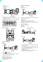
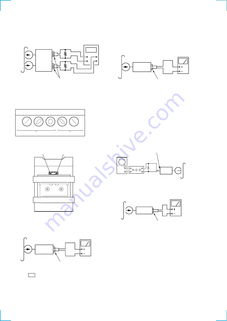
3. Phase check
Model: FWD playback
test tape
P-4-A100
(10kHz, –10dB)
R-CH
L-CH
set
47kW
47kW
oscilloscope
AUX OUT
(on ST-SP55)
V
H
4. Perform steps 1 to 3 in the FWD playback mode.
5. Confirm that phase error between L-ch and R-ch is in the range
of same phase to 90 degrees.
6. After the adjustments, apply suitable locking compound to the
parts adjusted.
Adjustment Location:
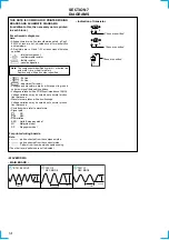
Waveform of oscilloscope
in phase
45
°
90
°
135
°
180
°
good
wrong
Tape Speed Adjustment
Procedure:
1. Insert the WS-48B into deck.
2. Press the
H
button of deck.
3. Adjust RV362 of the MAIN board so that the reading of the
frequency counter becomes 3000 ± 90 Hz.
Adjustment Location:
MAIN board
Sample Value of Wow and flutter
W.RMS (JIS) less than 0.3%
(test tape: WS-48B)
test tape
WS-48B
(3kHz, 0dB)
set
AUX OUT
(on ST-SP55)
level meter
Adjust RV211 (L-CH) and RV261 (R-CH), so that adjustment within
the following adjustment level.
Adjustment level:
AUX OUT level: –8.2
±
0.5 dB (285 to 319 mV)
Level difference between the channels: within
±
1.0 dB
Confirm that the AUX OUT level does not change even though
play and stop are repeated.
Playback Level Adjustment
Procedure:
Mode: FWD playback
test tape
P-4-L300
(315Hz, 0dB)
set
AUX OUT
(on ST-SP55)
level meter
Record Bias Adjustment
Procedure:
1. Record mode.
AF OSC
AUX IN (on ST-SP55)
1) 315 Hz
2) 10 kHz
blank tape
CS-123
set
attenuator
600
Ω
} 50 mV (–23.8 dB)
2. Playback mode.
3. Confirm playback the signal recorded in step 1 become adjust-
ment level as follows.
Note:
You had better to refer “4-1-4. TC REC START POINT”
See page 9) when this adjustment
4. If these levels do not adjustment level, adjust the RV311 (L-CH)
and RV361 (R-CH), to repeat steps 1 to 3.
Adjustment level:
The playback outpout of 10 kHz level difference adjust
315 Hz reference should be 0 dB ± 0.5 dB.
recorded
position
set
AUX OUT
(on ST-SP55)
level meter
Adjustment scerw
(FWD mode)
Adjustment scerw
(REV mode)
Содержание CMT-SP55TC
Страница 18: ...CDP SP55 17 17 5 4 SCHEMATIC DIAGRAM BD SECTION See page 14 for Waveforms See page 20 for IC Block Diagrams ...
Страница 20: ...CDP SP55 19 19 5 6 SCHEMATIC DIAGRAM MAIN SECTION See page 21 for IC Block Diagrams ...
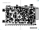
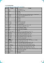
Страница 60: ...ST SP55 6 6 3 3 SCHEMATIC DIAGRAM MAIN SECTION Page 8 Page 8 Page 8 PIN FUNCTION ...
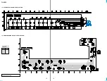
Страница 62: ...ST SP55 8 8 3 5 SCHEMATIC DIAGRAM PANEL SECTION Page 6 Page 6 Page 6 LCD BACK LIGHT ...
Страница 102: ...8 MEMO ...
Страница 105: ...TA SP55 11 11 4 3 SCHEMATIC DIAGRAM MAIN SECTION ...
Страница 107: ...TA SP55 13 13 4 5 SCHEMATIC DIAGRAM PANEL SECTION ...
Страница 131: ...CDP SP55 17 17 5 4 SCHEMATIC DIAGRAM BD SECTION See page 14 for Waveforms See page 20 for IC Block Diagrams ...
Страница 133: ...CDP SP55 19 19 5 6 SCHEMATIC DIAGRAM MAIN SECTION See page 21 for IC Block Diagrams ...
Страница 146: ...ST SP55 6 6 3 3 SCHEMATIC DIAGRAM MAIN SECTION Page 8 Page 8 Page 8 PIN FUNCTION ...
Страница 148: ...ST SP55 8 8 3 5 SCHEMATIC DIAGRAM PANEL SECTION Page 6 Page 6 Page 6 LCD BACK LIGHT ...

