9
4-1-4. TC REC START POINT
Procedure:
1. Set the test mode, and press the REC button (TC) and then the
H
button (TC) to set the recording state.
2. Pressing the CD SYNC REC button (TC) returns to the starting point of recording.
SECTION 4
TEST MODE
4-1.
TEST MODE FOR NOT CONNECTING THE WHOLE SYSTEM
(When connecting TA-SP55,ST-SP55,TC-SP55)
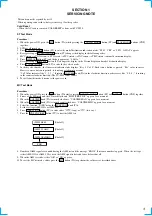
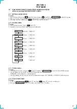
4-1-1. SETTING THE TEST MODE
Procedure:
1. When the power ON, press the
?/1
button (TA) while pressing the
s
button (TC) and CD SYNC REC buttons (TC) together.
2. When the test mode is set, the PAUSE LED will light up for 0.1 seconds at intervals of 3.2 seconds.
3. To exit the test mode, either press the
?/1
button (TA) and turn OFF the power.
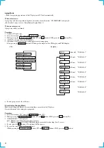
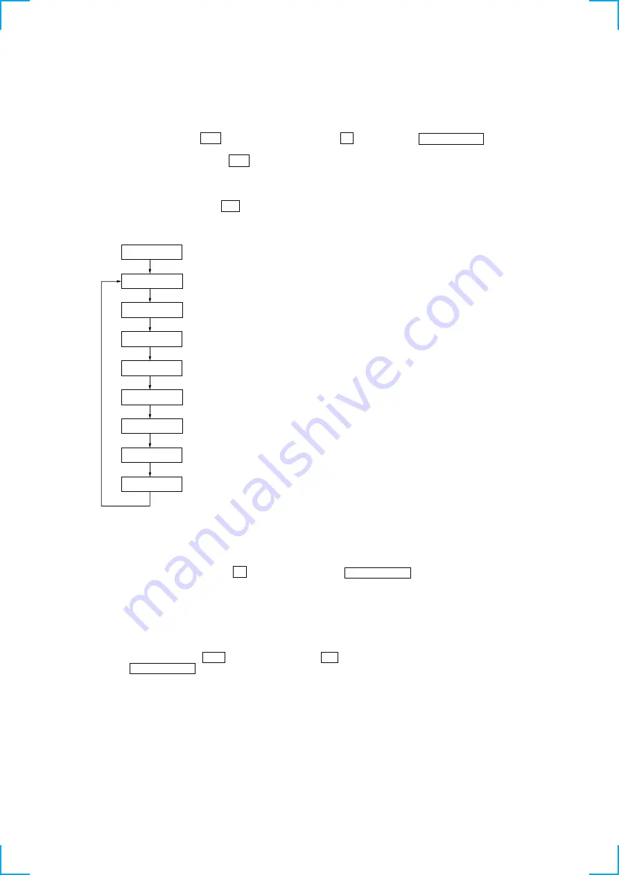
4-1-2. TC AGING MODE
Procedure:
1. After setting the test mode, press the
H
button (TC).
2. Operations are performed in the following sequence during aging.
REW
(Shut off)
"TAPE AG-1"
FWD
FF
REV
REW
(20 sec)
"TAPE AG-2"
(20 sec)
"TAPE AG-3"
(20 sec)
"TAPE AG-4"
(20 sec)
(20 sec)
(20 sec)
"TAPE AG-5"
FF search
REW search
OPEN
CLOSE
"TAPE AG-6"
"TAPE AG-7"
"TAPE AG-8"
"TAPE AG-9"
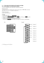
4-1-3. TC AMS CHECK
Procedure:
1. After setting the test mode, pressing the
s
button (TC) and then the CD SYNC REC button (TC) will start REW operations.
2. After rewinding to the tape top,FF search in the FWD direction starts.
“TAPE EDG*” will be displayed.(*: Arbitrary number)
3. After FF searching to the tape end, the tape will be automatically stopped, and “TAPE OK” or “TAPE NG” will be displayed.
Содержание CMT-SP55TC
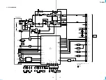
Страница 18: ...CDP SP55 17 17 5 4 SCHEMATIC DIAGRAM BD SECTION See page 14 for Waveforms See page 20 for IC Block Diagrams ...
Страница 20: ...CDP SP55 19 19 5 6 SCHEMATIC DIAGRAM MAIN SECTION See page 21 for IC Block Diagrams ...
Страница 60: ...ST SP55 6 6 3 3 SCHEMATIC DIAGRAM MAIN SECTION Page 8 Page 8 Page 8 PIN FUNCTION ...
Страница 62: ...ST SP55 8 8 3 5 SCHEMATIC DIAGRAM PANEL SECTION Page 6 Page 6 Page 6 LCD BACK LIGHT ...
Страница 102: ...8 MEMO ...
Страница 105: ...TA SP55 11 11 4 3 SCHEMATIC DIAGRAM MAIN SECTION ...
Страница 107: ...TA SP55 13 13 4 5 SCHEMATIC DIAGRAM PANEL SECTION ...
Страница 131: ...CDP SP55 17 17 5 4 SCHEMATIC DIAGRAM BD SECTION See page 14 for Waveforms See page 20 for IC Block Diagrams ...
Страница 133: ...CDP SP55 19 19 5 6 SCHEMATIC DIAGRAM MAIN SECTION See page 21 for IC Block Diagrams ...
Страница 146: ...ST SP55 6 6 3 3 SCHEMATIC DIAGRAM MAIN SECTION Page 8 Page 8 Page 8 PIN FUNCTION ...
Страница 148: ...ST SP55 8 8 3 5 SCHEMATIC DIAGRAM PANEL SECTION Page 6 Page 6 Page 6 LCD BACK LIGHT ...

