5
Aging Mode
• Mode for repeating operations of the CD player and TC deck automatically.
When errors occur:
Aging stops and a message indicating that an error has occurred such as “CD MEC ERR” is displayed.
(For details of errors, refer to “Error History Display Mode”.)
When no errors occur:
Aging is repeatedly performed.
Procedure:
1. Load any CD and a tape.
2. Select the function “ CD ” using the FUNCTION knob (TA).
3. While pressing the TUNING MODE button (ST) and
H
button (CDP), press the
?
/
1
button (TA).
4. “AGING” is displayed on the fluorescent display tube briefly.
5. Operations are performed in the following sequence during aging.
Every pressing of DISPLAY button (ST) changes the display in the CD display and TAPE display.
6.
To end aging, execute the cold reset.
Error History Display Mode
Mode for checking the history of errors which have occurred in the CD player.
Execute this mode after ending the aging mode.
Procedure:
1.
Select the function “ CD ” using the FUNCTION knob (TA).
2.
While pressing the TUNING MODE button (ST) and
S
button (CDP), press the
?
/
1
button (TA).
3.
“EMC@@EDC**” id displayed.
@@ : Number of mechanism errors (Last 3 errors)
**
: Number of errors (NO DISC ERROR) which occurred after chucking (Last 3 errors)
4.
To end, press the
?
/
1
button (TA) and turn OFF the power.
Note:
To erase the error history, perform cold reset.
(While pressing the TUNING MODE button (ST) and
ML
button (CDP), press the
?
/
1
button (TA).)
CD :
Cassette :
Reading of TOC
Playback of first track (3sec.)
Playback of last track (3sec.)
CD tray open
CD tray close
REW
(Shut off)
"TAPE AG-1"
PLAY
FF
REV PLAY
REW
(2 min)
"TAPE AG-2"
(Shut off)
"TAPE AG-3"
(2 min)
"TAPE AG-4"
(Shut off)
"TAPE AG-5"
(Shut off)
"TAPE AG-6"
(Shut off)
"TAPE AG-7"
"TAPE AG-8"
"TAPE AG-9"
(Shut off)
FF
REW
OPEN
CLOSE
Содержание CMT-SP55TC
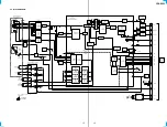
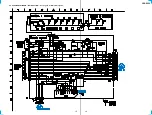
Страница 18: ...CDP SP55 17 17 5 4 SCHEMATIC DIAGRAM BD SECTION See page 14 for Waveforms See page 20 for IC Block Diagrams ...
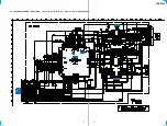
Страница 20: ...CDP SP55 19 19 5 6 SCHEMATIC DIAGRAM MAIN SECTION See page 21 for IC Block Diagrams ...
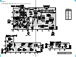
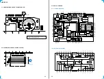
Страница 60: ...ST SP55 6 6 3 3 SCHEMATIC DIAGRAM MAIN SECTION Page 8 Page 8 Page 8 PIN FUNCTION ...
Страница 62: ...ST SP55 8 8 3 5 SCHEMATIC DIAGRAM PANEL SECTION Page 6 Page 6 Page 6 LCD BACK LIGHT ...
Страница 102: ...8 MEMO ...
Страница 105: ...TA SP55 11 11 4 3 SCHEMATIC DIAGRAM MAIN SECTION ...
Страница 107: ...TA SP55 13 13 4 5 SCHEMATIC DIAGRAM PANEL SECTION ...
Страница 131: ...CDP SP55 17 17 5 4 SCHEMATIC DIAGRAM BD SECTION See page 14 for Waveforms See page 20 for IC Block Diagrams ...
Страница 133: ...CDP SP55 19 19 5 6 SCHEMATIC DIAGRAM MAIN SECTION See page 21 for IC Block Diagrams ...
Страница 146: ...ST SP55 6 6 3 3 SCHEMATIC DIAGRAM MAIN SECTION Page 8 Page 8 Page 8 PIN FUNCTION ...
Страница 148: ...ST SP55 8 8 3 5 SCHEMATIC DIAGRAM PANEL SECTION Page 6 Page 6 Page 6 LCD BACK LIGHT ...

