background image

1-1

CDP-D12

Section 1

Service Overview

1-1. Installation

1-1-1. Operating Environment

Operation temperature :

+

d

C to 

+

40 

d

C

(Functions guaranteed)

Storage temperature :

_

20 

d

C to 

+

60 

d

C

Mass :

Approx. 4.0 kg

Power supply voltage :

AC 100 V (for J)
AC 120 V (for UC)
AC 230 V (AC 220 V to 240 V)
(for CE)
AC 220 V (for CN)

Power supply frequency : 50/60 Hz (for J/CE/CN)

60 Hz (for UC)

Power consumption :

16 W (for J and CE)
18 W (for UC and CN)

1-1-2. Installation Space

Do not install in the following places:

.

Areas exposed to direct sunlight or other strong light

.

Dusty areas

.

Areas with strong electric or magnetic fields

.

Areas near heat sources

.

Areas subject to vibration

.

Areas with much electrical noise

.

Areas with much static noise

Note for installation

The unit has been designed to be used upright. Therefore
do not place it on its side nor tilt it.

c

Laser beam

When servicing, do not approach the laser exit with the eye
too closely. In case it is necessary to confirm laser beam
emission, be sure to observe from a distance of more than
30 cm from the surface of the objective lens on the optical
pick-up block.

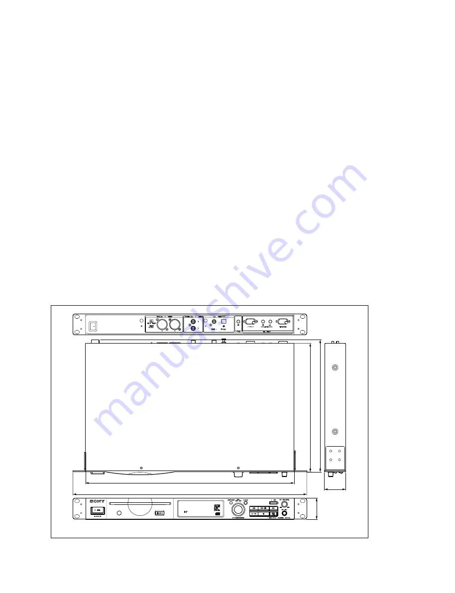
44

265

272

44

482

430

Unit : mm

Содержание CDP-D12

Страница 1: ...COMPACT DISC PLAYER CDP D12 SERVICE MANUAL 1st Edition ...

Страница 2: ...den Um die Gefahr eines elektrischen Schlages Feuergefahr und Verletzungen zu vermeiden sind bei Wartungsarbeiten strikt die Angaben in der Anleitung zu befolgen Andere als die angegeben Wartungsarbeiten dürfen nur von Personen ausgeführt werden die eine spezielle Befähigung dazu besitzen AVERTISSEMENT Ce manual est destiné uniquement aux personnes compétentes en charge de l entretien Afin de rédu...

Страница 3: ... length 780 nm Emission duration Continuous Laser output power 30 mW max CAUTION Use of controls or adjustments or performance of procedures other than those specified herein may result in hazardous radiation exposure DANGER INVISIBLE LASER RADIATION WHEN OPEN AVOID DIRECT EXPOSURE TO BEAM DANGER RADIATIONS INVISIBLES DU LASER EN CAS D OUVERTURE EVITER TOUTE EXPOSITION DIRECTE AU FAISCEAU This lab...

Страница 4: ......

Страница 5: ...net 1 4 1 3 1 Cover 1 4 1 3 2 Front Panel 1 5 1 4 Replacement of Main Parts 1 5 1 4 1 Removing and Installing the CD Mechanism Deck Assembly MG 398SC 121 and Internal Parts 1 5 1 4 2 Replacing the Power Fuse 1 11 1 5 How to Eject a Disc in the Case of Emergency 1 11 1 6 Initializing the Setups 1 12 1 7 Mounting Screw of the RS 232C and PARALLEL Connectors 1 12 1 8 Unleaded Solder 1 12 2 Spare Part...

Страница 6: ... CDP D12 5 Board Layouts AC SW 5 1 DISPLAY 5 1 EJECT 5 1 HP 5 1 MAIN 5 2 POWER 5 4 LOAD 5 5 SENSOR 5 5 SERVO 5 5 SW 5 5 6 Schematic Diagrams MAIN 6 1 LOAD 6 3 SENSOR 6 3 SERVO 6 3 SW 6 3 Frame Wiring 6 4 ...

Страница 7: ...ce Service Center Operating Instructions Supplied with CDP D12 This manual describes how to operate the CDP D12 Semiconductor Pin Assignments CD ROM Available on request This Semiconductor Pin Assignments CD ROM allows you to search for semiconductors used in B P Company equipment Semiconductors that cannot be searched for on this CD ROM are listed in the service manual for the corresponding unit ...

Страница 8: ...Contains information on semiconductors used for the unit It includes a complete list of the semiconductors and their ID Nos for retrieving information on Semiconductor Pin Assignments CD ROM which is available separately Please refer to this section together with the Semiconductor Pin Assignments CD ROM Information on the semiconductors not contained in the CD ROM at the time of issue of this manu...

Страница 9: ...the following places Areas exposed to direct sunlight or other strong light Dusty areas Areas with strong electric or magnetic fields Areas near heat sources Areas subject to vibration Areas with much electrical noise Areas with much static noise Note for installation The unit has been designed to be used upright Therefore do not place it on its side nor tilt it c Laser beam When servicing do not ...

Страница 10: ... Male 1 568 182 11 connector 1 766 771 11 shell RELAY IN OUT Stereo mini jack Stereo mini plug SONY RK G136 or equivalent RS232C D sub 9 pin Male D sub 9 pin Female 1 568 181 11 connector 1 563 375 11 shell CTRL S Mini jack φ3 5 Control S connecting cable Accessory of CDP D12 OPTICAL Square optical Optical digital connecting _ connector cable COAXIAL Pin jack Pin plug _ ANALOG OUTPUT UNBAL Pin jac...

Страница 11: ... signal output of the AES EBU format Output level _18 dBm radiating wavelength 660 mm DIGITAL OUT COAXIAL Phone jack Digital audio signal output of the AES EBU format Output leve l 0 5 Vp p 20 Load impedance 75 Z ANALOG OUT UNBAL L R Phone jack Analog audio signal output unbalanced Maximum output level 8 dBu 0 dBu 0 775 Vrms Load impedance 10 kZ or more ANALOG OUT BAL L R XLR type 3 pins male Anal...

Страница 12: ...ng the parts replacement turn off the power and disconnect the plug from the outlet 1 3 1 Cover 1 Remove the eight screws BVTT3 x 8 and remove the rack mount bracket 2 Remove the four screws case M3 x 8 remove the three step tapping screws M3 x 8 and remove the cover in the direction of the arrow BVTT3 x 8 BVTT3 x 8 Cover Rack mount bracket Rack mount bracket Screws case M3 x 8 Screws case M3 x 8 ...

Страница 13: ...placement turn off the power and disconnect the plug from the outlet 1 4 1 Removing and Installing the CD Mechanism Deck Assembly MG 398SC 121 and Internal Parts 1 CD mechanism deck assembly MG 398SC 121 1 Remove the cover and the front panel Refer to 1 3 Removing the Cabinet 2 Disconnect the harness from the connector CN3 on the AC SW board 3 Remove the four screws BVTT3 x 5 and remove the chassi...

Страница 14: ...nd remove the chassis T388 assembly in the direction of the arrow in the way of disengaging the claws 4 Remove the SERVO board and the guide DISC M Refer to item 3 of Section 1 4 1 5 Install the SERVO board and the guide DISC M removing the step 3 in the new chassis T388 assem bly Refer to item 3 of Section 1 4 1 6 Install the chassis T388 assembly by reversing steps 1 to 3 of removal PTT2 6 x 6 P...

Страница 15: ... item 1 of Section 1 4 1 n If the chassis T388 assembly is still installed when removing the SERVO board remove soldering of the chassis T388 assembly Refer to item 2 of Section 1 4 1 2 Remove soldering of the LO motor assembly at the two positions 3 Remove soldering of the SERVO board at the two positions 4 Disconnect the two cables from the connectors CN2 CN3 on the SERVO board 5 Remove the thre...

Страница 16: ...all the new LO motor sub assembly by reversing the steps of removal 6 Arm roller assembly 1 Remove the CD mechanism deck assembly Refer to item 1 of Section 1 4 1 2 Remove the chassis T388 assembly Refer to item 2 of Section 1 4 1 3 Remove the tension coil spring RA 4 Remove the arm roller assembly in the direction of the arrow 5 Install the new arm roller assembly by reversing the steps of remova...

Страница 17: ...on 1 4 1 4 Remove the LO motor assembly Refer to item 5 of Section 1 4 1 5 Remove the tension coil spring KF1 from the protruded portion of the floating block assembly 6 Remove the three dampers T 7 While pulling the lever D in the direction of arrow A rotate the loading ring in the direction of arrow B and release the lock 8 Remove the floating block assembly in the direction of arrow C n When th...

Страница 18: ...ism deck assembly Refer to item 1 of Section 1 4 1 2 Remove the chassis T388 assembly Refer to item 2 of Section 1 4 1 3 Remove the SERVO board Refer to item 4 of Section 1 4 1 4 Remove the LO motor assembly Refer to item 5 of Section 1 4 1 5 Remove the floating block assembly Refer to item 8 of Section 1 4 1 6 Remove the sled motor assembly Refer to item 9 of Section 1 4 1 7 Disconnect the pickup...

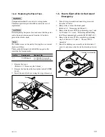
Страница 19: ...the cover Refer to 1 3 Removing the Cabinet 2 Remove the fuse from the fuse holder on the POWER board 3 Install the new fuse by reversing the steps of removal Fuse POWER bpard Fuse holders 1 5 How to Eject a Disc in the Case of Emergency 1 Turn off the power and disconnect the power cord from the AC outlet 2 Remove the cover and the front panel Refer to 1 3 Removing the Cabinet 3 Remove the chassi...

Страница 20: ...areful 1 6 Initializing the Setups Various setups can be initialized to the default setups when shipped from the factory as follows 1 Turn off the POWER switch 2 While pressing the STOP key and the MENU EXIT button at the same time turn on the POWER switch 3 The message Factory Preset appears on the display and various setups are initialized to the default setups automatically 4 The initialization...

Страница 21: ...rts 3 Stock of Parts Parts marked with o at SP Supply Code column of the spare parts list may not be stocked Therefore the delivery date will be delayed 4 Harness Harnesses with no part number are not registered as spare parts In need of repair get components shown in the list and repair using them 5 Destination Representation The part indicated For UC CE CN in the spare parts list is used in the ...

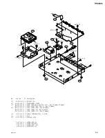
Страница 22: ...ON 4 2 338 688 01 s SCREW STEP TAPPING 5 2 346 661 11 s BUTTON P 6 2 347 869 01 s PLATE WINDOW 7 2 347 872 01 s FILTER IR 8 2 347 875 01 s BUTTON AMS 9 2 347 878 01 s BRACKET RACK MOUNT 10 2 347 881 01 s BUTTON EJECT No Part No SP Description 11 3 367 431 01 s KNOB BAL 12 3 704 366 01 s SCREW CASE M3X8 EP FE ZNBK 13 4 942 568 41 s EMBLEM N0 5 SONY 14 4 951 620 01 s SCREW 2 6X8 BVTP TAPPING ST 15 4...

Страница 23: ...532 215 00 s FUSE TIME LAG 0 8A 250V L 20 For CE model CN model 1 533 449 11 s FUSE GLASS TUBE DIA 5 For UC model 104 1 696 169 12 s CORD POWER AEP For CE model 1 782 510 11 s CORD POWER CN For CN model 1 738 531 11 s CORD POWER U C For UC model 105 1 827 545 11 s CABLE FLEXIBLE FLAT 30 CORE 106 3 670 155 11 s FOOT 107 4 217 350 01 s STOPPER CORD 7 682 946 09 s SCREW PSW 3X5 7 685 647 79 s SCREW B...

Страница 24: ...5 A 4591 506 A s MOUNTED CIRCUIT BOARD SENSOR 206 A 4591 507 A s MOUNTED CIRCUIT BOARD SW LOAD 207 X 3378 870 4 s CHASSIS T388 ASSY 208 3 032 474 11 s GUIDE DISC M 209 3 039 629 01 o BRACKET MOTOR 210 3 040 022 01 s RETAINER RA SHAFT 211 3 040 034 01 s SPRING RA TENSION 212 3 040 040 21 s ARM ROLLER 213 3 040 042 01 s WASHER 214 3 040 044 01 s ROLLER S 215 3 043 880 01 s RING RA RETAINING PETP 216...

Страница 25: ...1 s WHEEL U WORM 305 3 014 727 01 s WHEEL LW WORM 306 3 018 272 01 s WASHER 307 3 040 026 01 s SPRING CH TENSION 308 3 040 031 01 s DAMPER T 309 3 040 032 01 s SPRING FL COMPRESSION 310 3 040 033 01 s SPRING KF1 TENSION 311 3 048 258 01 s SPRING 8 K 312 3 220 180 01 s SPRING TR2 TENSION 313 3 913 404 01 s RETAINER DISC 314 3 931 881 11 s LEVER LOCK 315 3 931 882 02 s GEAR MDL 316 3 931 894 01 s BR...

Страница 26: ...ED CIRCUIT BOARD SW LIMIT 404 X 3378 961 1 s SERVICE ASSY CHASSIS OP 405 1 676 707 11 s PWB PICK UP FLEXIBLE 406 1 823 951 11 s FLEXIBEL FLAT CABLE 6P 407 3 040 029 01 s SPRING SL TORSION 408 3 040 030 01 s SPRING FEED PLATE 409 3 040 045 01 s BASE DRIVING 410 3 040 194 01 s GEAR SL MIDWAY 411 3 909 607 01 s SCREW 412 8 820 165 06 s DEVICE OPTICAL KSS 721A C RP 7 627 553 37 s SCREW PRECISION P 2X3...

Страница 27: ... KEYBOARD S710 1 473 779 11 s ENCODER ROTARY SWITCH EJECT BOARD Ref No or Q ty Part No SP Description C792 1 131 992 11 s CAP CERAMIC 100000PF F 1608 C793 1 131 992 11 s CAP CERAMIC 100000PF F 1608 CN791 1 568 942 11 o PIN CONECTOR 4P IC702 8 749 016 97 s IC NJL62H400A R790 1 216 809 11 s RESISTOR CHIP 100 1 10W 1608 R792 1 216 805 11 s RESISTOR CHIP 47 1 10W 1608 S791 1 762 875 21 s SWITCH KEYBOA...

Страница 28: ...ITOR ELECT 22MF 63V C221 1 126 934 11 s CAPACITOR ELECT 220MF 16V MAIN BOARD Ref No or Q ty Part No SP Description C228 1 126 768 11 s CAPACITOR ELECT 2200MF 16V C251 1 128 858 11 s CAPACITOR ELECT 22MF 50V AU C252 1 119 824 11 s CAPACITOR ELECT 10MF 50V C253 1 137 503 11 s CAPACITOR FILM 100PF 100V PP C254 1 162 215 31 s CAPACITOR CERAMIC 47PF 50V SL C255 1 127 725 91 s CAPACITOR ELECT 220MF C256...

Страница 29: ...409 8 719 921 63 s DIODE MTZJ 7 5B D512 8 719 109 97 s DIODE RD6 8ES B2 D601 8 719 977 12 s DIODE DTZ6 8B D602 8 719 109 97 s DIODE RD6 8ES B2 D603 8 719 109 97 s DIODE RD6 8ES B2 D604 8 719 109 97 s DIODE RD6 8ES B2 MAIN BOARD Ref No or Q ty Part No SP Description D605 8 719 109 97 s DIODE RD6 8ES B2 D606 8 719 109 97 s DIODE RD6 8ES B2 D607 8 719 083 69 s DIODE UDZSTE 1724B D608 8 719 083 69 s D...

Страница 30: ... 3 9K 1 4W MAIN BOARD Ref No or Q ty Part No SP Description R158 1 215 435 00 s RESISTOR METAL FILM 3 9K 1 4W R159 1 215 435 00 s RESISTOR METAL FILM 3 9K 1 4W R160 1 215 435 00 s RESISTOR METAL FILM 3 9K 1 4W R161 1 215 440 00 s RESISTOR METAL FILM 6 2K 1 4W R162 1 215 441 00 s RESISTOR METAL FILM 6 8K 1 4W R163 1 215 477 00 s RESISTOR METAL FILM 220K 1 4W R164 1 215 441 00 s RESISTOR METAL FILM ...

Страница 31: ... R619 1 216 827 11 s RESISTOR CHIP 3 3K 1 10W 1608 R620 1 249 417 11 s RESISTOR CARBON 1K 1 4W SMALL R621 1 249 417 11 s RESISTOR CARBON 1K 1 4W SMALL R622 1 216 827 11 s RESISTOR CHIP 3 3K 1 10W 1608 R623 1 249 417 11 s RESISTOR CARBON 1K 1 4W SMALL R624 1 249 417 11 s RESISTOR CARBON 1K 1 4W SMALL R625 1 216 827 11 s RESISTOR CHIP 3 3K 1 10W 1608 MAIN BOARD Ref No or Q ty Part No SP Description ...

Страница 32: ...s CAPACITOR CHIP CERAMIC 0 1MF C20 1 107 826 11 s CAPACITOR CHIP CERAMIC 0 1MF C21 1 162 970 11 s CAPACITOR CERAMIC 0 01MF 25V B C22 1 162 970 11 s CAPACITOR CERAMIC 0 01MF 25V B C23 1 162 970 11 s CAPACITOR CERAMIC 0 01MF 25V B C24 1 162 970 11 s CAPACITOR CERAMIC 0 01MF 25V B C25 1 162 970 11 s CAPACITOR CERAMIC 0 01MF 25V B C30 1 162 970 11 s CAPACITOR CERAMIC 0 01MF 25V B C34 1 162 970 11 s CA...

Страница 33: ...AME Ref No or Q ty Part No SP Description 1pc 1 443 084 11 s TRANSFORMER POWER 1pc 1 532 215 00 s FUSE TIME LAG 0 8A 250V for CE CN 1pc 1 533 449 11 s FUSE GLASS TUBE DIA 5 for J UC 1pc 1 696 169 12 s CORD POWER for CE 1pc 1 738 531 11 s CORD POWER for UC 1pc 1 782 510 11 s CORD POWER for CN 1pc 1 824 534 11 s CORD POWER TRACKING for J 1pc 8 820 165 06 s DEVICE OPTICAL KSS 721A C RP HN101 1 827 54...

Страница 34: ......

Страница 35: ...e when a part is to be replaced also refer to the Spare Parts section In addition for semiconductors with ID Nos refer to the separate CD ROM titled Semiconductor Pin Assignments Sony Part No 9 968 546 xx that allows searching for parts by semiconductor type or ID No The semiconductors in the manual or on the CD ROM are listed by equivalent types Thus the external view or the index mark indication...

Страница 36: ...VIDER AND SELECTION CIRCUITRY ICLK 1 S1 S0 4 5 2 CLK CLK 2 8 7 BR9040F WE2 ROHM ICS541MT ICS EMITTER CPT 230S C TD BC SANYO IC 1 2 3 4 5 6 7 8 MCLK BICK SDTI LRCK PDN CSN CCLK CDTI 16 15 14 13 12 11 10 9 DZFL DZFR VCC GND AOUTL AOUTL_ AOUTR AOUTR_ 2 CHANNEL AUDIO D A CONVERTER TOP VIEW INPUTS BICK CCLK CDTI CSN LRCK MCLK PDN SDTI OUTPUTS AOUTL AOUTL_ AOUTR AOUTR_ DZFL DZFR AUDIO SERIAL DATA CLOCK ...

Страница 37: ...IFIER NON REVERSE CHANNEL AMPLIFIER REVERSE LOADING DRIVER REVERSE CHANNEL AMPLIFIER LOADING DRIVER POSITIVE LOADING DRIVER NEGATIVE DRIVER CHANNEL POSITIVE DRIVER CHANNEL NEGATIVE BIAS MUTE CONTROL CHANNEL POWER SUPPLY PREVIOUS LOADING POWER SUPPLY POWER SAVE CONTROL PIN NO 1 2 3 4 5 6 7 8 9 10 11 12 13 14 I O SIGNAL PIN NO 15 16 17 18 19 20 21 22 23 24 25 26 27 28 I O SIGNAL FWD REV LDCONT PS IN...

Страница 38: ... INTERFACE DRAM RAS CONTROL DRAM WE CONTROL AUDIO SERIAL LR CLOCK AUDIO SERIAL BIT CLOCK MICROCONTROLLER INTERFACE STATUS AUDIO SERIAL DATA DRAM DATA MICROCONTROLLER INTERFACE EXTENSION SUPPLY CONTROL INPUT2 YDMUTE RESET TEST CONTROL INPUT1 OUTPUT INTERFACE GENERAL PORT MICRO CONROLLER INTERFACE ATTENUATOR YBLKCK YFCLK YFLAG ZLRCK ZSCK ZSRDATA YMDATA YMCLK YMLD ZSENSE DIT UC1 UC5 CLK RAS CAS CAS2 ...

Страница 39: ... GND D VCC DA GND DA VCC EQ1 EQ2 X GND X VCC RF SIGNAL AFTER GAIN ADJUSTMENT TEST C1 ERROR CORRECT RESULT C2 ERROR CORRECT RESULT BUFFER FOR OSCILLATOR CLOCK DAC FOR ADJUSTMENT SERIAL SOUND DATA EFM SIGNAL PRE EMPHASIS FOCUS DRIVE FLAG DEFECT DETECT L CHANNEL SOUND DATA LD CONTROL CURRENT EFM SYNCHRONIZATION DETECT L CHANNEL AUDIO DISTINGUISH SOUND DATA TO R CHANNEL AND L CHANNEL SPINDLE DRIVE MIR...

Страница 40: ...ODE SYNC MB90553APF G 250 BND TOP VIEW 81 85 90 95 100 50 45 40 35 31 80 75 70 65 60 55 51 1 5 10 15 20 25 30 PIN SIGNAL I O DESCRIPTION 56 PARA O PARALLEL PORT NO_DISC POWEROUT 57 PARA O PARALLEL PORT PLAY OUTPUT PLAYOUT 58 PARA O PARALLEL PORT PAUSE OUTPUT PAUSEOUT 59 PARA I PARALLEL PORT PLAY INPUT PLAYIN 60 PARA I PARALLEL PORT PAUSE INPUT PAUSEIN 61 CCL_FS O CLOCK CONTROLLER CLOCK 62 PARA I P...

Страница 41: ... OPT DIGTALOUT SW 4 10dB 768FS 384FS IC253 IC153 IC121 IC103 IC503 IC502 Q601 4MHz RECIVER SIRCS CTRL S RELAY I O RC232 DECK MECHA MG 398SC IC402 DIVIDER IC405 KEY IC702 IC602 IC601 IC901 FL IC501 IC102 CONVERTER P A IC101 PLL E2PROM DRAM IC404 IC403 PROOF SHOCK 604 603 Q602 602 PH601 PLL IC401 CONTROL SYSTEM decoded and receives the error correction in the digital signal processing block The audi...

Страница 42: ......

Страница 43: ...for CE CN 32 for J AC SW A SIDE Component side B SIDE Solder Pattern SUFFIX 12 for UC 22 for CE CN 32 for J DISPLAY A SIDE Component side B SIDE Solder Pattern SUFFIX 12 EJECT B SIDE Solder side B SIDE Solder Pattern SUFFIX 12 HP A SIDE Component side B SIDE Solder Pattern SUFFIX 12 for UC 22 for CE CN 32 for J CN7 C N 7 8 2 FLK1 S701 S702 S703 S704 S705 S706 S707 S708 S709 S 7 1 0 DISPLAY B SIDE ...

Страница 44: ...5 2 CDP D12 5 2 MAIN MAIN MAIN A SIDE Component side B SIDE Solder Pattern SUFFIX 12 for UC 22 for CE CN 32 for J ...

Страница 45: ... 0 2 I C 5 0 3 I C 6 0 1 I C 6 0 2 I C 9 0 1 J R 4 0 1 J R 6 0 1 Q 2 1 Q 2 2 Q 2 3 Q 2 5 Q 4 0 1 Q 6 0 1 Q 6 0 2 Q 6 0 3 Q 6 0 4 Q 6 0 5 Q 6 0 6 Q 6 1 0 Q 6 1 1 Q 6 9 1 R 1 0 2 R 1 0 3 R 1 0 4 R 1 0 7 R 1 0 8 R 1 0 9 R 1 1 0 R 1 1 1 R 1 1 2 R 1 1 3 R 1 1 4 R 1 1 7 R 1 1 8 R 1 1 9 R 1 2 0 R 1 2 1 R 1 2 2 R 1 2 3 R 2 0 2 R 2 0 3 R 2 0 4 R 2 0 7 R 2 0 8 R 2 0 9 R 2 1 0 R 2 1 1 R 2 1 2 R 2 2 1 R 2 2 2...

Страница 46: ...der side B SIDE Solder Pattern SUFFIX 12 for UC POWER A SIDE Component side B SIDE Solder Pattern SUFFIX 12 for UC POWER A SIDE Component side B SIDE Solder Pattern SUFFIX 22 for CE CN POWER B SIDE Solder side B SIDE Solder Pattern SUFFIX 32 for J POWER A SIDE Component side B SIDE Solder Pattern SUFFIX 32 for J ...

Страница 47: ... Pattern SUFFIX 11 SW A SIDE Component side B SIDE Solder Pattern SUFFIX 11 SERVO B SIDE SUFFIX 11 SW B SIDE Solder side B SIDE Solder Pattern SUFFIX 11 SENSOR B SIDE Solder side B SIDE Solder Pattern SUFFIX 11 LOAD B SIDE Solder side B SIDE Solder Pattern SUFFIX 11 LOAD A SIDE Component side B SIDE Solder Pattern SUFFIX 11 ...

Страница 48: ......

Страница 49: ...Q601 Q610 Q611 Q691 Q602 Q603 Q604 Q605 Q606 L601 L602 R440 R446 R447 R448 R679 C437 C438 J601 R455 R404 R647 R460 R680 R681 J603 J604 D691 D692 L106 C110 R408 R415 R426 CN901 IC601 C420 C503 IC101 R417 C419 IC602 R113 R114 R803 R626 R627 R628 R612 R611 R615 R614 R618 R617 R630 R629 R621 R624 R620 R806 R805 C518 R419 C501 C502 C611 C612 C613 C614 C615 C661 C662 C665 C901 C902 C903 C904 C905 CN602 ...

Страница 50: ... A 3300 35V 220 16V 100 25V 220p 25V 220 16V NJM78M05DL1A NM 11ES2 TA1B 22 25V 470 50V 3 3 50V 470p 50V 470p 50V 0 1 25V 220p 25V 220p 25V 470p 50V 470p 50V 220p 25V 220p 25V 1SS133T 1SS133T 1SS133T 0 0 0 0 4P EP892 R463 Q21 Q22 D408 C36 IC24 C23 CN151 R157 R167 R261 R122 R222 R223 R156 R255 R256 R161 R162 R158 R159 R160 R164 R163 R257 R258 R262 R263 R259 R260 R265 R266 R267 C153 R264 R456 R24 R25...

Страница 51: ...B1197K 16P 0 0 CPT 230S C TU CPT 230S C TU CPT 230S C TU RST D_SW SELF_SW PH1 IN_SW PH3 TSI TSO TSCK STB A0 RFOK RFCK SBSY RAM_OVER RAM_OVER EJECT D_DATA BCK LRCK D_DATA BCK LRCK RFCK SBSY PH3 TSI TSO TSCK STB A0 RST RFOK LOAD SL SL SP SP LD LD D_SW SELF_SW IN_SW TD FD MD SD IN_SW PH1 PD LD LD D B C A PD F E EJECT LOAD FCS FCS TRK TRK MD SD TD FD TSCK TSI F E C D A B TRK TRK FCS LD LD SP SP SL SL ...

Страница 52: ...ND HP_R 2 2 2 2 3 4 2 3 4 2 3 4 2 3 4 2 3 4 2 3 4 1 2 3 4 5 6 7 8 9 10 11 12 13 14 15 16 17 18 19 20 21 22 23 24 25 26 27 28 29 30 LIMIT D_SW SELF_SW PH1 INSW PH2 PH3 DR 6 7V DR 6 7V DR_GND DR_GND EJECT LOAD SBSY RFCK LRCK BCK D_DATA RAM_OVER 384FS D_5V D_GND TDSPSI TDSPSO TSCK STB A0 CD_RST RFOK A_GND A_5V 1 2 3 4 5 6 7 8 9 10 11 12 13 14 15 16 17 18 19 20 21 22 23 24 25 26 27 28 29 30 LIMIT D_SW...

Страница 53: ... commercial leakage tester such as the Simpson 229 or RCA WT 540A Follow the manufacturers instructions to use these instruments 2 A battery operated AC milliammeter The Data Precision 245 digital multimeter is suitable for this job 3 Measuring the voltage drop across a resistor by means of a VOM or battery operated AC voltmeter The limit indication is 0 75 V so analog meters must have an accurate...

Страница 54: ...Printed in Japan Sony Corporation 2003 10 16 2003 CDP D12 UC CE CN E 9 976 920 01 ...

Отзывы: